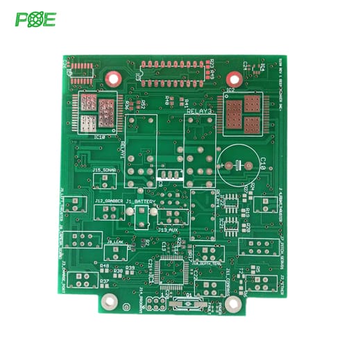
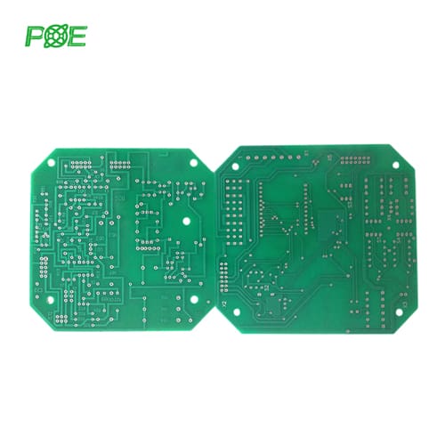
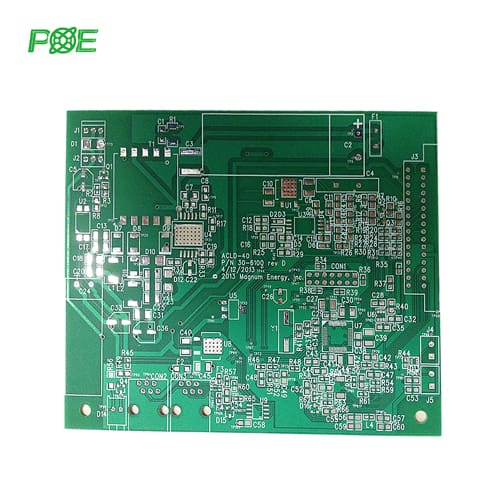
Layers
2 layers (top and bottom)
Material
FR-4, High-Tg FR-4, Rogers, PTFE, Aluminum substrate, etc.
Board Thickness
0.2mm – 3.2mm
Copper Thickness
0.5 Oz (17.5 µm) – 4 Oz (140 µm)
Minimum Hole Size
0.15mm-0.25mm (6mil-10mil)
Minimum Trace/Space Width
3mil/3mil (0.0762mm/0.0762mm)
Aspect Ratio
10:1 or better
Maximum Board Size
500mm x 1100mm (20" x 44")
Surface Finish
HASL, Lead-Free HASL, ENIG, Immersion silver, OSP, Hard Gold, etc.
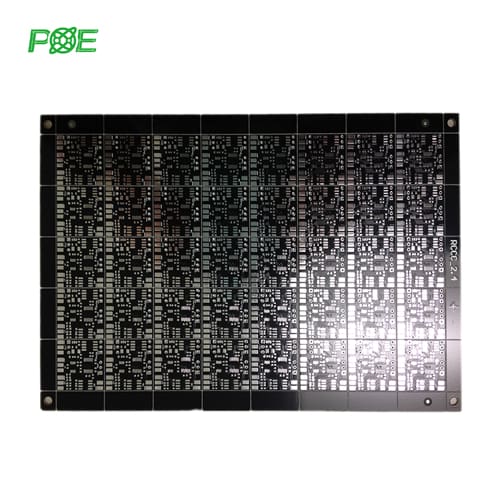
Solder Mask
Green, Blue, Yellow, Black, Red, White, and other colors
Solder Mask Resolution
4mil (0.1mm) minimum
Solder Mask Registration
±2mil (±0.0508mm)
Silkscreen Color
White, Black, Yellow, and other colors
Plated Through Holes (PTH)
Yes
Blind & Buried Vias (BBV)
No
Electrical Testing
Continuity & isolation, impedance control
Certification
ISO9001:2015;ISO13485:2016;ROHS,UL 94v0, IPC-600G classll and IPC-6012B classll standard

 Email: all@poe-pcba.com
 Whatsapp: 85292069596
 Tel: 0755-25312250/ +8613798543496
 Factory Address: Floor 3, Jinyuan Industrial Park, No. 56, Tangtou Avenue, Shiyan Town, Baoan District, Shenzhen China