Layers
1-40+ layers (Specialized RF designs with mixed dielectric materials)
Assembly Type
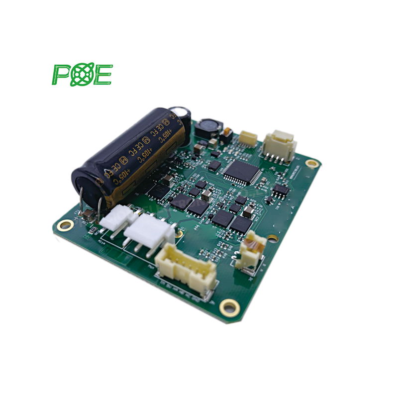
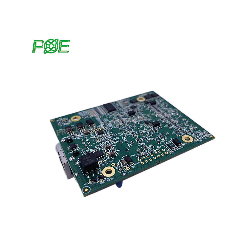
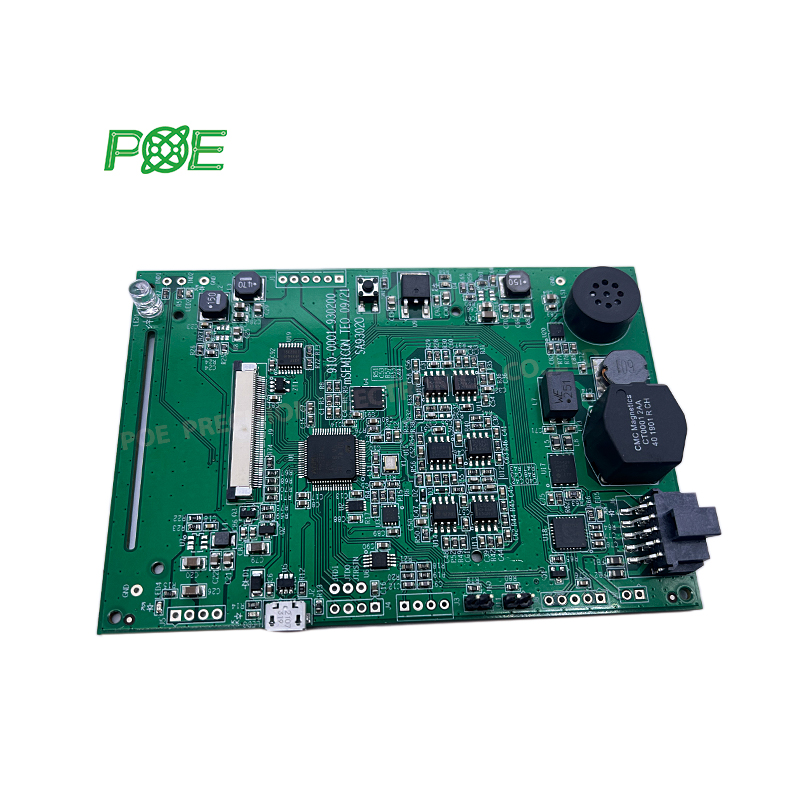
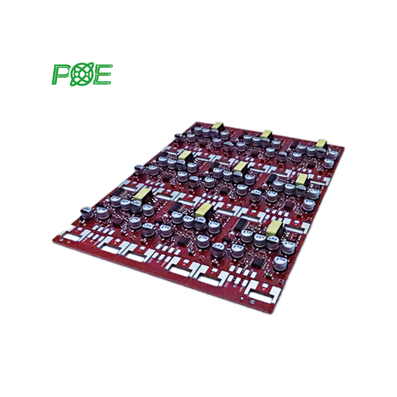
Through-Hole (THT), Surface Mount (SMT), Mixed (THT+SMT)
Minimum Component Size
01005 (Imperial) / 0402 (Metric) - Critical for high-density RF designs
Maximum Component Size
50 mm × 50 mm × 10 mm (2.0 in × 2.0 in × 0.4 in)
Component Package Types
BGA, QFN, QFP, SOIC, SOP, SSOP, TSSOP, PLCC, DIP, RF-specific packages
Minimum Pad Pitch
0.4 mm (16 mil) for BGA, 0.5 mm (20 mil) for QFP/QFN
Minimum Trace Width
0.075 mm (3 mil) - Essential for RF transmission lines
Minimum Trace Spacing
0.075 mm (3 mil) - Critical for impedance control
Minimum Drill Size
0.15 mm (6 mil)
Maximum Board Size
457 mm × 610 mm (18 in × 24 in)
Maximum Board Thickness
1.6 mm to 3.2 mm (0.062 in to 0.125 in)
Board Material
Rogers (RO4350B, RO4003C, RT/Duroid 5880), PTFE, FR-4, High-Tg FR-4, Taconic, Isola, Aluminum, Flexible(FPC), Rigid-Flex
Frequency Range
DC-40GHz (Depending on material and design)
Impedance Control
±5%, ±7%, ±10% (Single-ended and Differential)
Dielectric Constant (Dk) Range
2.2-10.2 (Material-dependent)
Loss Tangent (Df) Range
0.001-0.025 (Material-dependent)
Surface Finish
ENIG (Preferred for RF), HASL, OSP, Immersion Silver, Gold Finger
Solder Paste Type
Leaded or Lead-Free (RoHS Compliant)
Assembly Process
Reflow Soldering, Wave Soldering, Hand Soldering, Vapor Phase Soldering
Shielding Capabilities
EMI/RFI Shielding, Compartmental Shielding, Conformal Coating
Inspection Methods
Automated Optical Inspection (AOI), X-ray, Visual Inspection
Testing Methods
Vector Network Analyzer (VNA) up to 20GHz, S-Parameter Testing, In-Circuit Test (ICT), Functional Test (FCT), Flying Probe Test
Design for Manufacturing (DFM)
RF-specific DFM Analysis and Feedback, Signal Integrity Analysis
Turnaround Time
Prototype: 24 hours to 7 days, Production: 10 days to 4 weeks
PCB Assembly Standards
ISO9001:2015, ISO13485:2016, ROHS, UL 94V0, IPC-600G Class II, IPC-6012B Class II, IPC-A-610 Class 3
RF Design Support
Microstrip/Stripline Design, Controlled Impedance Routing, RF Layout Optimization

 Email: all@poe-pcba.com
 Whatsapp: 85292069596
 Tel: 0755-25312250/ +8613798543496
 Factory Address: Floor 3, Jinyuan Industrial Park, No. 56, Tangtou Avenue, Shiyan Town, Baoan District, Shenzhen China