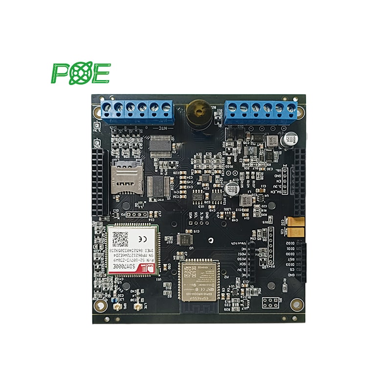
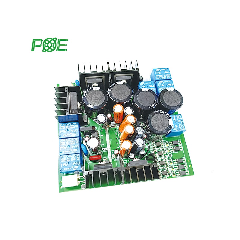
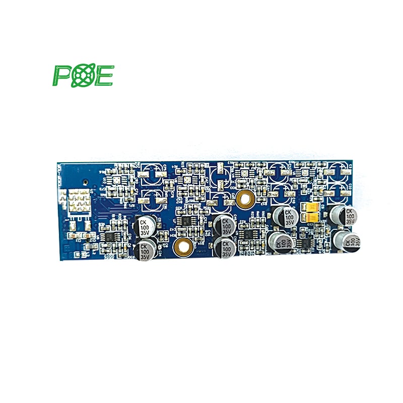
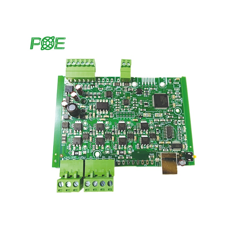
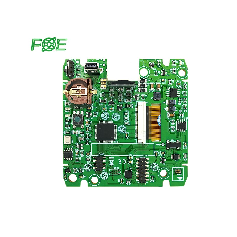
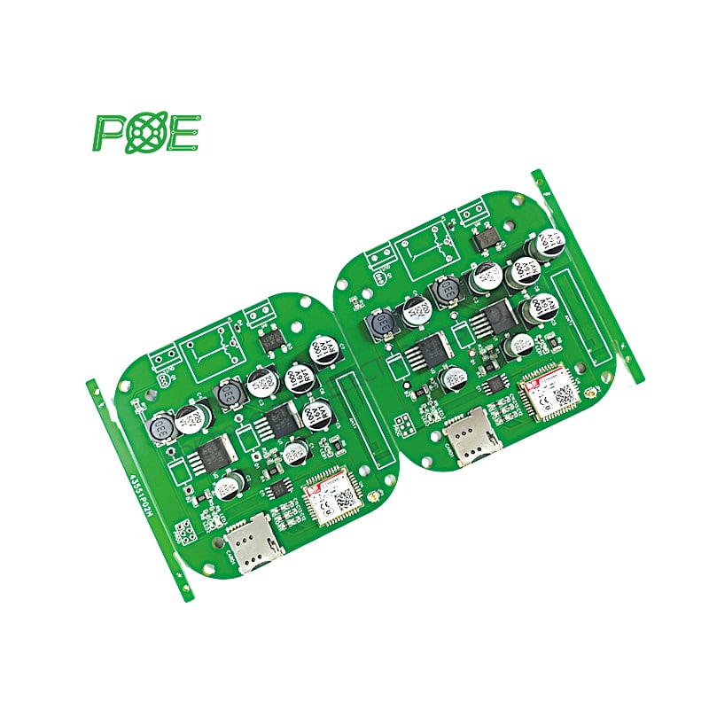
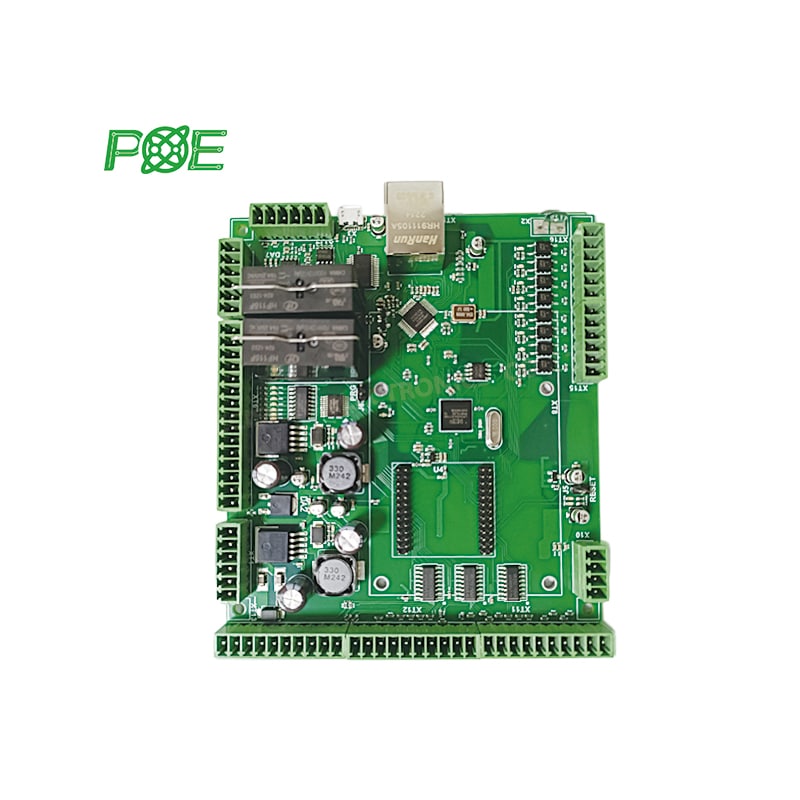
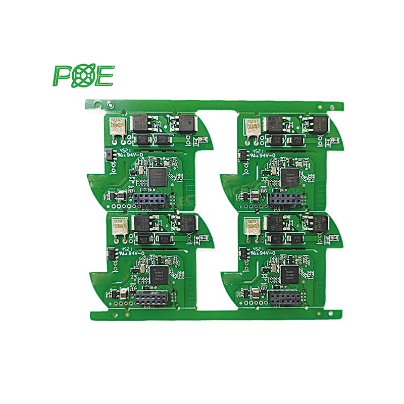
Assembly Type
Through-Hole (THT), Surface Mount (SMT), Mixed (THT+SMT)
Minimum Component Size
01005 or 0201 (Imperial) / 0402 or 0603 (Metric)
Maximum Component Size
2.0 in x 2.0 in x 0.4 in (50 mm x 50 mm x 10 mm)
Component Package Types
BGA, QFN, QFP, SOIC, SOP, SSOP, TSSOP, PLCC, DIP, etc.
Minimum Pad Pitch
0.5 mm (20 mil) for QFP, QFN, 0.8 mm (32 mil) for BGA
Minimum Trace Width
0.10 mm (4 mil)
Minimum Trace Spacing
0.10 mm (4 mil)
Minimum Drill Size
0.15 mm (6 mil)
Maximum Board Size
18 in x 24 in (457 mm x 610 mm)
Maximum Board Thickness
0.062 in (1.6 mm) to 0.125 in (3.2 mm)
Board Material
FR-4, High-Tg FR-4, Aluminum, High Frequency, Flexible(FPC), Rigid-Flex, Rogers, etc.
Surface Finish
HASL, Immersion Gold, Gold Finger, OSP, Immersion Silver, etc.
Solder Paste Type
Leaded or Lead-Free
Assembly Process
Reflow Soldering, Wave Soldering, Hand Soldering
Inspection Methods
Automated Optical Inspection (AOI), X-ray, Visual Inspection
Testing Methods
In-Circuit Test (ICT), Functional Test (FCT), Flying probe test
Design for Manufacturing (DFM)
DFM Analysis and Feedback
Turnaround Time
Prototype: 24 hours to 7 days, Production: 10 days to 4 weeks
PCB Assembly Standards
ISO9001:2015;ISO13485:2016;ROHS,UL 94v0, IPC-600G classll and IPC-6012B classll standard

 Email: all@poe-pcba.com
 Whatsapp: 85292069596
 Tel: 0755-25312250/ +8613798543496
 Factory Address: Floor 3, Jinyuan Industrial Park, No. 56, Tangtou Avenue, Shiyan Town, Baoan District, Shenzhen China