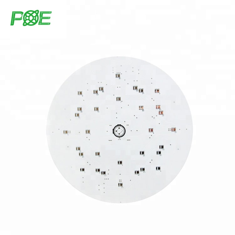
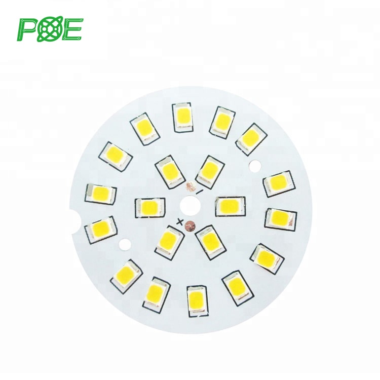
Technology Highlights
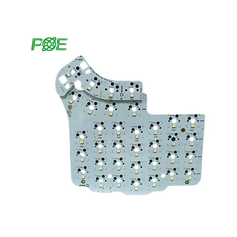
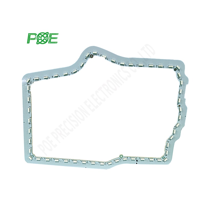
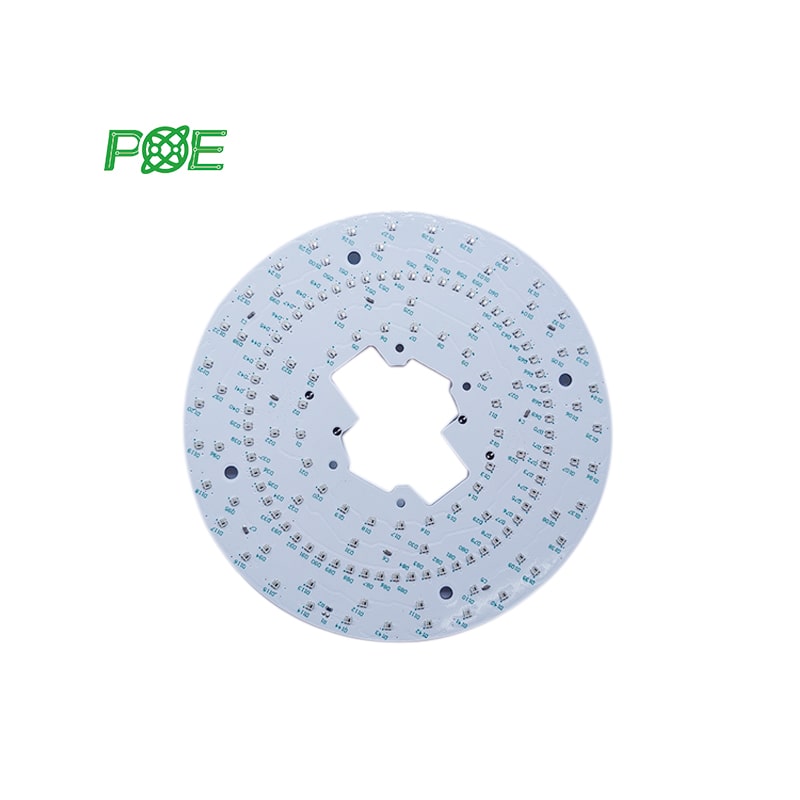
Advanced aluminum core with high thermal conductivity (≥220 W/m·K), suitable for high-power LED applications, automotive electronics, and power converters
Layer Count
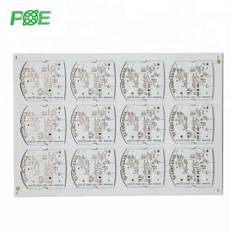
1-4 layers standard, up to 8 layers hybrid aluminum substrate available
Base Material
Premium-grade aluminum core with high thermal conductivity dielectric
Aluminum Type
Standard, high performance, halogen-free options available
Board Thickness
0.4mm - 3.2mm (±0.1mm tolerance)
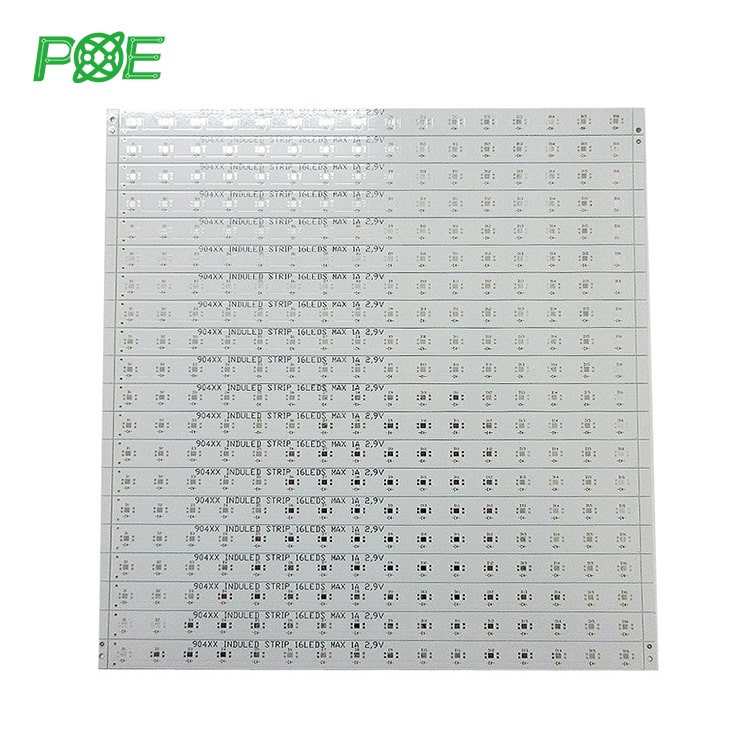
Maximum Dimensions
610mm × 450mm (precision laser drilling capability)
Copper Weights (Finished)
0.5 oz - 10.0 oz (inner and outer layers)
Minimum Track/Gap
0.075mm/0.075mm (3mil/3mil)
Surface Finishes
HASL, Lead-Free HASL, ENIG (immersion gold), ENEPIG, Immersion Silver, Immersion Tin, OSP, Gold Fingers
Solder Mask Colors
Green, Red, Yellow, Blue, White, Black, Purple (custom colors available)
Via Process Options
Tented vias, plugged vias, open vias (non-covered)
Thermal Performance
Superior heat dissipation, thermal resistance as low as 0.4°C/W
Special Features
Countersunk holes, castellated edges, heavy copper capability, mixed technology
Quality Standards
ISO 9001, UL Certified, RoHS & REACH Compliant, IPC-A-600 Class 2/3
Lead Time
Standard: 5-7 working days; Expedited: 3-4 working days (subject to complexity)

 Email: all@poe-pcba.com
 Whatsapp: 85292069596
 Tel: 0755-25312250/ +8613798543496
 Factory Address: Floor 3, Jinyuan Industrial Park, No. 56, Tangtou Avenue, Shiyan Town, Baoan District, Shenzhen China