
1–40 layer PCBs with blind/buried vias, impedance control, and HDI capability — prototype to mass production, IPC Class 2/3 certified.
| Specification | Details |
|---|---|
| Board Type | Rigid PCB · Flexible PCB · Rigid-Flex PCB · HDI PCB · Heavy Copper PCB · MCPCB · High-Frequency PCB (1–40 layers) |
| Materials | FR-4 · High Tg FR-4 · Rogers · Teflon · Aluminum · Polyimide |
| Board Dimensions | Min: 10×10mm — Max: 609×889mm |
| Board Thickness | 0.2mm — 6.0mm (common: 0.8mm, 1.6mm) |
| Min Line Width / Spacing | 50μm / 50μm (common: 100μm / 100μm) |
| Copper Thickness (Outer) | 0.5 oz — 10 oz (17μm — 345μm) |
| Copper Thickness (Inner) | 0.5 oz — 4 oz (17μm — 140μm) |
| Surface Finish | HASL · Lead-free HASL · ENIG · Immersion Silver · Immersion Tin · OSP · Hard Gold · Electrolytic Nickel Gold |
| Solder Mask | LPI (Liquid Photo-Imageable) · Dry Film |
| Solder Mask Colors | Green · Blue · Red · White · Black · Matte variants |
| Silkscreen Colors | White · Black · Yellow |
| Min Drill Size | 0.15mm (CNC) · 0.1mm (Laser blind/buried vias) |
| Drill Tolerance | ±0.05mm (standard) · ±0.025mm (advanced) |
| Aspect Ratio | Up to 20:1 |
| Impedance Control | Standard: ±10% · Advanced: ±5% (50Ω and below: ±5Ω) |
| Gold Finger Beveling | 30° · 45° · custom angles on request |
| Quality Standards | ISO 9001:2015 · ISO 13485:2016 · ISO 14001:2015 · RoHS · UL 94V-0 · IPC-A-600 · IPC-6012 |
| Turnaround Time | Standard: 5–10 days · Rush: 24 hours (subject to complexity) |
| Specification | Details |
|---|---|
| Layer Count | General PCB: 2–40 layers · HDI (7+N+7): staggered and stacked vias · Buried IC: supported |
| HDI Structure | HDI 1–7 steps · Blind/buried vias · Laser micro-vias · Any-layer HDI |
| Max Board Size | 508×889mm (20×35 inch) |
| Board Thickness | 0.21mm — 6.0mm |
| Min Track / Spacing | Inner layer: 2mil / 2mil · Outer layer: 2mil / 2mil |
| Outer Copper Thickness | Up to 8 oz |
| Inner Copper Thickness | Up to 8 oz |
| Aspect Ratio | Up to 12:1 (standard) · 20:1 (advanced) |
| Min Annular Ring | Via: 3mil · Component hole: 5mil |
| Plug Via Hole | Min: 0.15mm (CNC) · 0.1mm (Laser) · Max: 0.7mm |
| Min SM Bridge (Green) | 3mil |
| Min SM Bridge (Black) | 4mil |
| Impedance Tolerance | ±10% standard · 50Ω and below: ±5Ω |
| V-Cut | CNC V-cut: 20° / 30° / 45° / 60° |
| Dimension Tolerance | ±0.1mm |
| Board Thickness Tolerance | 0.21–1.0mm: ±0.1mm · 1.0–2.5mm: ±7% · 2.5–6.3mm: ±6% |
| Finished Hole Tolerance | 0–0.3mm: ±0.08mm · 0.31–0.8mm: ±0.08mm · 0.81–1.60mm: ±0.05mm |
| X-Ray Inspection | Available for all HDI and BGA boards |
| Specification | Details |
|---|---|
| Base Material | FR-4 (Shengyi) · High Tg (Tg-220) · Halogen-free · PTFE · Polyimide · Rogers · Isola |
| PCB Types | Rigid PCB · FPC (Flexible) · Rigid-Flex · HDI |
| Max Layer Count | 40 layers |
| Min Base Copper | 1/3 oz (12μm) |
| Max Finished Copper | 10 oz |
| Min Trace/Spacing | Inner: 2/2mil (H/H oz base) · Outer: 2/2mil (1/3 oz base) |
| Min BGA Diameter | 8mil |
| Min BGA Pitch | 0.4mm |
| Min Hole Size | 0.15mm (CNC) · 0.1mm (Laser blind/buried) |
| Max Aspect Ratio | 20:1 |
| Min Insulating Layer | 2mil |
| Min SM Bridge | 3mil |
| Circuit Processing | Film · LDI (Laser Direct Imaging) |
| HDI & Special Types | HDI (1–7 steps) · Rigid-Flex (2–16 layers) · High-frequency mix-pressing (2–20 layers) · Buried capacitance & resistance |
| Surface Finish | ENIG · HASL · Lead-free HASL · OSP · Immersion Sn · Immersion Ag · Hard Gold · Plating Silver |
| Max PCB Size | 609×889mm |
ISO 9001:2015 · ISO 14001:2015 · ISO 13485:2016 · RoHS · UL 94V-0 · IPC-A-600 Class 2/3 · IPC-6012B Class 2/3
Flying Probe Testing · AOI · Impedance Testing · X-Ray Inspection · Microsection Analysis · E-Test (100% continuity)
Statistical Process Control (SPC) · In-Process Quality Control (IPQC) · Final Quality Control (FQC) · Full traceability documentation
Full certification documentation available on request — COC, test reports, and material traceability for every order.
Learn More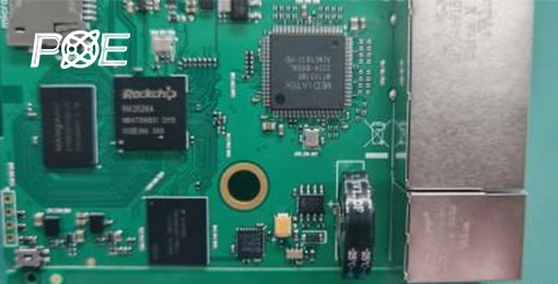
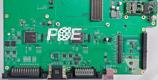
From bare PCB prototyping to PCBA sample production and planned bulk manufacturing transfer from Europe to China.
Advanced PCBA solutions for generalist superhumanoid robots capable of performing all core warehouse tasks.
Specialized PCB manufacturing with embedded copper coins for advanced research applications.
 Email: all@poe-pcba.com
 Whatsapp: 85292069596
 Tel: 0755-25312250/ +8613798543496
 Factory Address: Floor 3, Jinyuan Industrial Park, No. 56, Tangtou Avenue, Shiyan Town, Baoan District, Shenzhen China


