A full-capability PCB and PCBA manufacturing center in Shenzhen — serving medical, industrial, IoT, and telecommunications clients worldwide.
Click any step to see the equipment and process detail. Every board passes through the full sequence before leaving our facility.
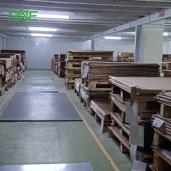
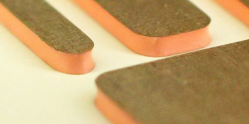
Premium FR4 substrate preparation and precision cutting. Material selection is the foundation of every high-quality PCB — we source only certified laminates that meet IPC standards.
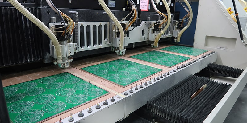
Multilayer PCB fabrication from 1 to 40 layers, supporting standard FR4, high-frequency Rogers, polyimide, and specialty substrates. From single prototype to mass production.
View Capabilities →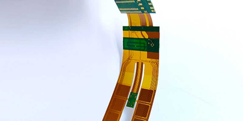
High Density Interconnect and rigid-flex PCB solutions for space-constrained applications. Blind and buried vias, via-in-pad, and laser drilling capabilities.
View Capabilities →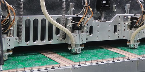
PCB prototypes from 24 hours, MOQ 1 piece. DFM review included on every order. Ideal for engineering validation before committing to production volumes.
View Capabilities →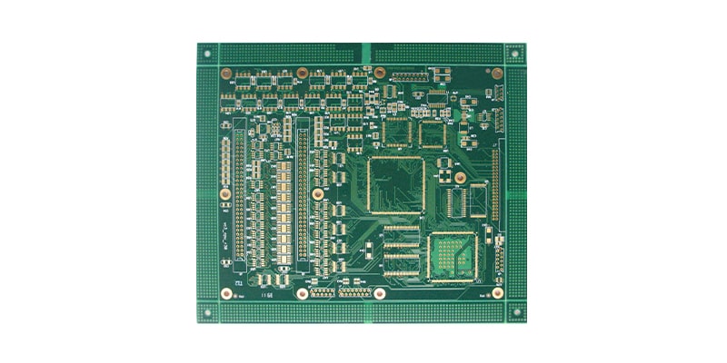
High Density Interconnect PCB manufacturing with microvias, stacked vias, and fine-pitch traces for compact, high-performance designs.
View Capabilities →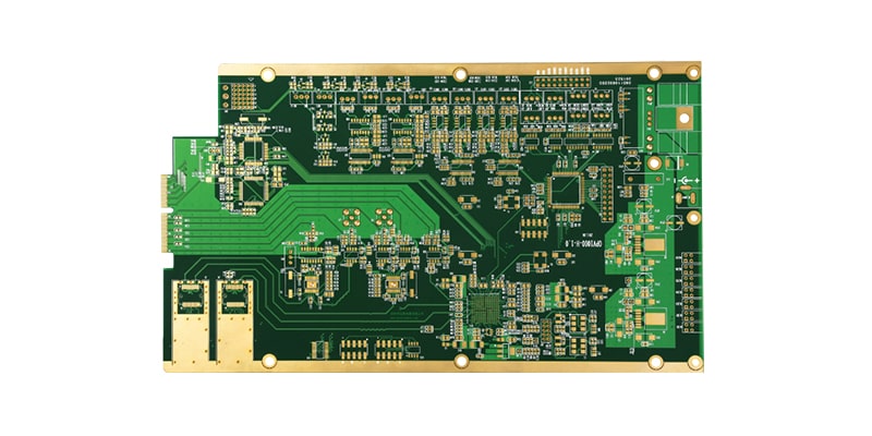
4 to 32 layer PCB fabrication with controlled impedance, tight registration, and consistent dielectric thickness across all layers.
View Capabilities →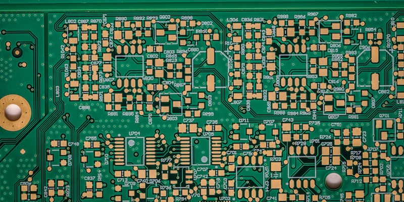
Controlled impedance PCBs for high-speed digital, RF, and microwave applications. Every impedance-critical board is tested and certified before shipment.
View Capabilities →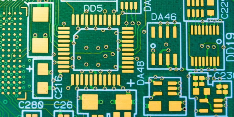
HASL, ENIG, Immersion Tin, Immersion Silver, OSP, Hard Gold, and Soft Gold. We recommend the right finish for your application and reliability requirements.
Electrical testing, AOI, X-ray inspection, and flying probe testing. Every board is verified against specification before leaving our facility.
View Quality →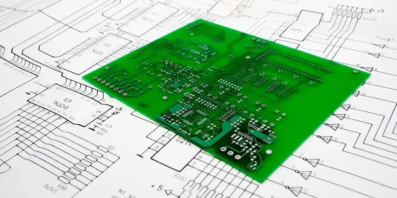
DFM analysis and PCB layout optimization on every order. Our engineers review your files before production and flag any issues that could affect yield or reliability.
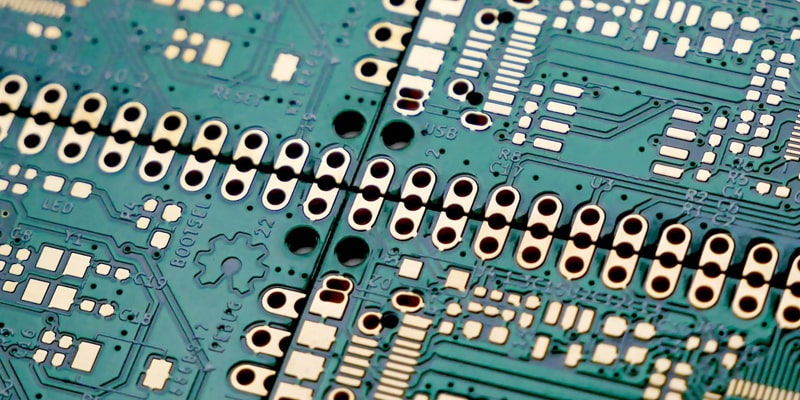
Via-in-pad and via filling technology for high-density designs. Resin-filled and copper-capped vias for BGA and fine-pitch component placement.
Heavy copper PCBs from 3.5 oz to 10 oz for power supply, automotive, and industrial applications requiring high current capacity and thermal management.
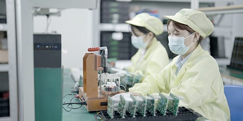
PCB fabrication, component sourcing, PCBA, and testing under one roof. No coordination overhead, no handoff delays.
35 dedicated procurement engineers. Competitive pricing through 10+ years of distributor relationships across China and internationally.
AOI, X-ray, flying probe, and electrical testing at every critical stage. 99.9% quality pass rate across all production runs.
Deep experience in medical devices, 5G, robotics, IoT, and power supply — industries where precision is non-negotiable.
Floor 3, Jingyuan Industrial Park
No.56 Tangtou Avenue
Shiyan Town, Bao'an District
Shenzhen, China
 Email: all@poe-pcba.com
 Whatsapp: 85292069596
 Tel: 0755-25312250/ +8613798543496
 Factory Address: Floor 3, Jinyuan Industrial Park, No. 56, Tangtou Avenue, Shiyan Town, Baoan District, Shenzhen China