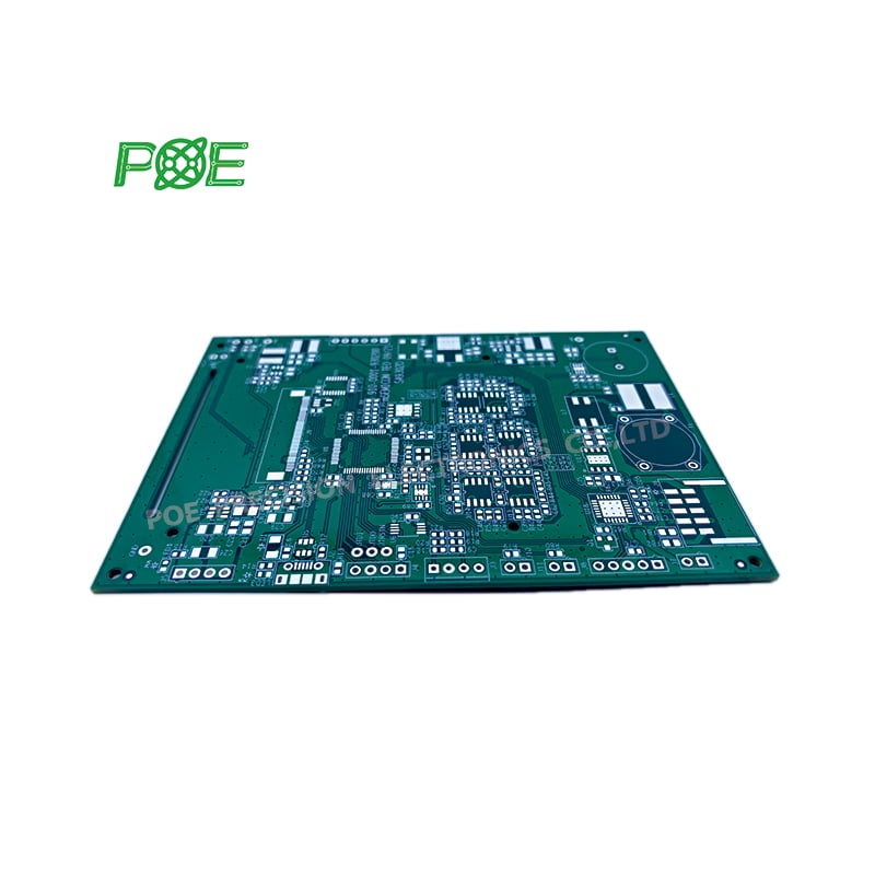
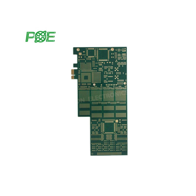
Layers
4 - 40+ layers, with various HDI structures including 1+N+1, 2+N+2, 3+N+3, and ELIC (Every Layer Interconnect) technology
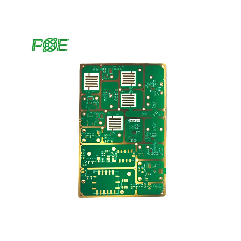
Material
FR-4, High Tg FR-4, Halogen-free, Rogers (RO4350B, RO3003), Isola
Board Thickness
0.2mm - 6.0mm with precise thickness control
Copper Thickness
0.5 oz - 6 oz (17.5μm - 210μm) with multi-level copper capability
Minimum Hole Size
0.1mm for mechanically drilled vias, 0.075mm for laser-drilled microvias with aspect ratio control
Minimum Trace/Space Width
Industry-leading capability of 2 mils (50μm) standard, with advanced capability down to 1 mil (25μm) for high-density designs
Via Technology
Blind/Buried vias, Stacked vias, Via-in-Pad (filled and plated), and Skip vias for optimal routing solutions
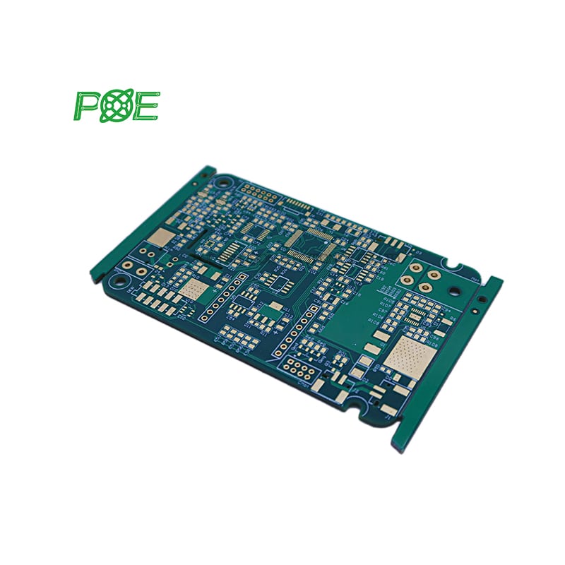
Solder Mask
LPI (Liquid Photo-Imageable) in Green, Yellow, White, Black, Blue, Red, and custom colors with ±1.0mil registration accuracy
Silkscreen
White, Black, Yellow, and custom colors with high-resolution printing capability
Surface Finishes
ENIG (3-5μin gold), OSP, Immersion Silver, Immersion Tin, HASL, and Hard Gold (30μin+) for specific applications
Minimum Annular Ring
2 mils (50μm) for outer layers, 1 mil (25μm) for inner layers, supporting high-reliability designs
Controlled Impedance
Tolerance of ±8% standard, with ±5% available for critical applications, verified by TDR testing
Special Features
Embedded passive components (resistors, capacitors), rigid-flex designs, back drilling, sequential lamination, and high-frequency material processing
Quality Assurance
100% electrical testing, impedance testing, cross-section analysis, and thermal stress testing
Certifications
ISO 9001, ISO 14001, UL, IPC-A-600 Class 2/3, RoHS and REACH compliant

 Email: all@poe-pcba.com
 Whatsapp: 85292069596
 Tel: 0755-25312250/ +8613798543496
 Factory Address: Floor 3, Jinyuan Industrial Park, No. 56, Tangtou Avenue, Shiyan Town, Baoan District, Shenzhen China