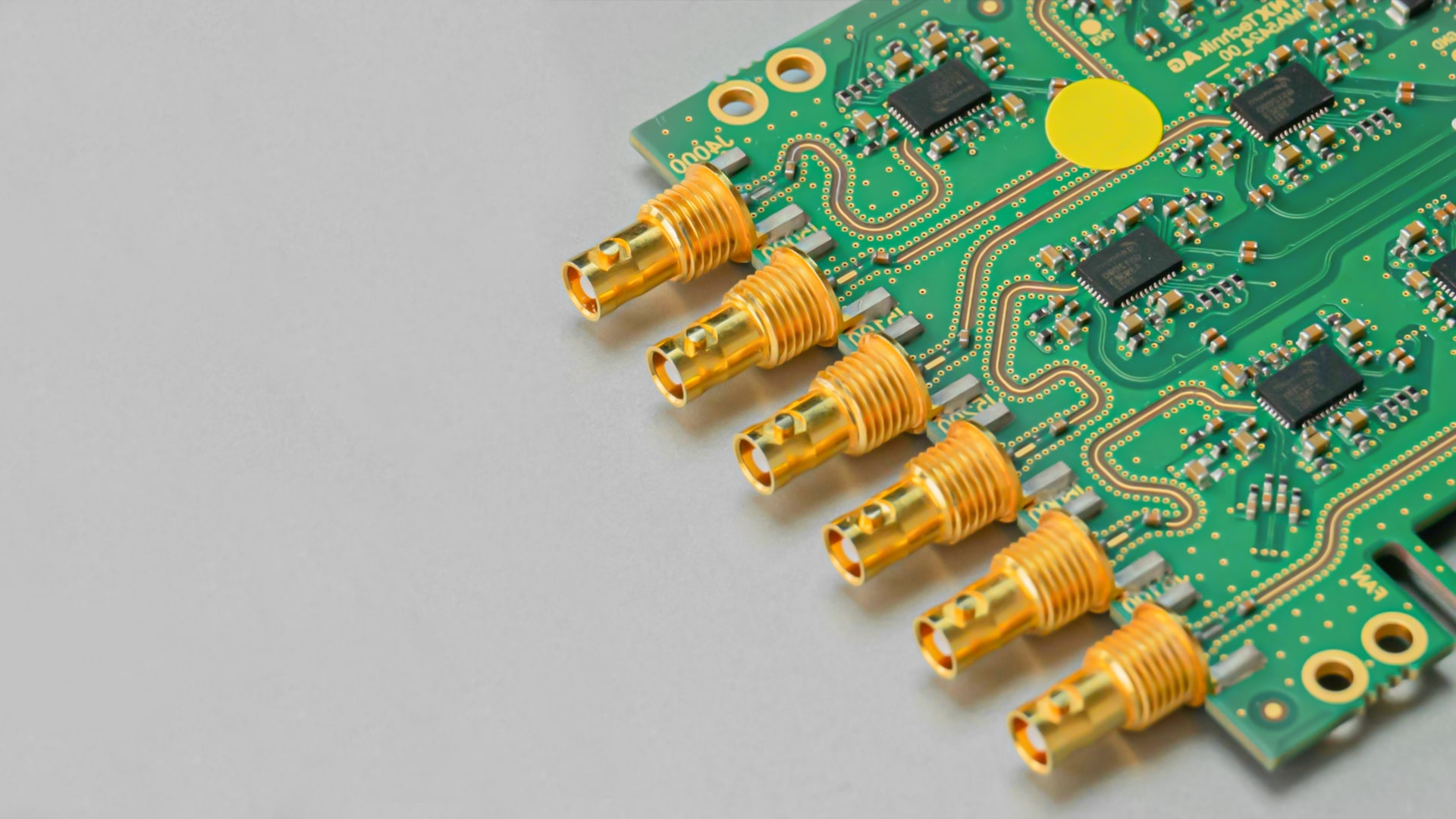
Web Analytics Made Easy - Statcounter
High Density Interconnect(HDI) PCB Manufacturing Services | POE
This website uses cookies:
Our website use cookies to analyze website accesses and improve your online experience. By continuing browsing this website,you agree to our use of cookies and privacy policy.
Accept all cookies
Decline
This website uses cookies:
Our website use cookies to analyze website accesses and improve your online experience. By continuing browsing this website,you agree to our use of cookies and privacy policy.
Accept all cookies
Decline
Get A Quote
Get A Quote
Worried About Surprise Tariffs? We Cover It, $0 to You.
×

HDI PCB

POE specializes in advanced HDI (High Density Interconnect) PCB fabrication with microvias, sequential lamination, and ultra-fine pitch capabilities since 2011. We manufacture 1+N+1 to 3+N+3 HDI structures with laser-drilled microvias down to 50μm, supporting complex multilayer designs for smartphones, tablets, wearables, and high-performance computing applications.

Our state-of-the-art facilities feature advanced laser drilling systems, precise sequential build-up processes, and comprehensive electrical testing to deliver HDI boards that meet the most demanding miniaturization and performance requirements.

Get A Quote

WHAT CAN POE
DO FOR YOUR HDI PCB?

Get A Quote

No MOQ,
24/7 engineering support

Quick-turn HDI PCB
prototypes in 5–7 days

1–100000 pcs
factory-direct pricing

4–20 layers HDI PCB
1+N+1 to 3+N+3 structures

Laser microvias, sequential lamination;
50μm via diameter capability

UL, ISO9001, ISO14001,
RoHS compliant

Free CAM/DFM review
before fabrication

Fast quotation and
reply within 4 hours

Advanced HDI processes:
stacked/staggered microvias

99.8%+ on‑time delivery and quality satisfaction

SHOWCASE
APPLICATIONS

Submit your HDI design files and stackup requirements, and POE will manufacture advanced HDI PCBs with precise microvia formation, sequential build-up layers, and ultra-fine pitch capabilities. We specialize in complex HDI structures including stacked microvias, skip vias, and any-layer HDI configurations for next-generation electronic devices requiring maximum miniaturization and performance.

Smartphones & Tablets HDI PCB
Smartphones & Tablets
Wearable Devices HDI PCB
Wearable Devices
High-Speed Computing HDI PCB
High-Speed Computing
5G Infrastructure HDI PCB
5G Infrastructure
Medical Implants HDI PCB
Medical Implants
Security Systems Rigid PCB
IoT Sensors
Telecom Rigid PCB
Automotive Electronics
Robotics Rigid PCB
AI Processors
RF & Wireless Rigid PCB
Millimeter Wave
HDI PCB application banner
Highlight image
Others:
Detail 1
Detail 2

POE HDI PCB
CAPABILITIES

Get A Quote
 
Specifications
POE's Bare Rigid PCB Capabilities
1
PCB Layers
4 to 20 layers HDI (1+N+1 to 3+N+3 structures)
2
Order Quantity
1–100000+ pcs
3
Lead Time
HDI Prototype 5–7 days; Production 7–18 days (depends on HDI complexity)
4
Material Options
Low‑loss dielectrics, Modified Epoxy, Polyimide, Low‑Dk/Df materials
5
Testing
100% E‑test, AOI, microvia inspection, impedance verification, cross‑section analysis
6
Board Thickness
0.4 mm to 2.0 mm (ultra‑thin HDI capability)
7
Min Trace/Space
1.6 mil / 1.6 mil (down to 25μm/25μm for advanced HDI)
8
Copper Weight
0.5 oz to 3 oz (higher available upon review)
9
Surface Finish
ENIG, Immersion Tin, Immersion Silver, HASL/Lead‑free HASL, OSP
10
Via Options
Laser microvias (50μm‑150μm), stacked/staggered vias, via‑in‑pad, copper‑filled microvias

HDI PCB
MANUFACTURING PROCESS

Get A Quote
01
Core substrate prep
Core substrate prep
02
Laser microvia drilling
03
Desmear & metallization
04
Build-up layer lamination
05
Sequential processing
06
Final surface finish
01
Core substrate prep
Core substrate prep
02
Laser microvia drilling
03
Desmear & metallization
04
Build-up layer lamination
05
Sequential processing
06
Final surface finish

FAQ

Still need help? Chat with us.

Get A Quote

What HDI structures can POE manufacture?

We manufacture 1+N+1 to 3+N+3 HDI structures with laser-drilled microvias, stacked and staggered configurations, skip vias, and any-layer HDI designs. Our advanced sequential build-up process supports complex multilayer HDI requirements.

What is the minimum microvia size you can achieve?

Our laser drilling systems can produce microvias as small as 50μm diameter with precise aspect ratios. We support copper-filled microvias, via-in-pad designs, and maintain tight tolerances for high-density interconnect applications.

What is the typical lead time for HDI PCBs?

HDI prototypes require 5–7 days due to sequential lamination processes, while production runs take 7–18 days depending on HDI complexity and layer count. Complex 3+N+3 structures may require additional time.

How do you ensure HDI quality and reliability?

We perform comprehensive testing including cross-section analysis, microvia inspection, impedance verification, and 100% electrical testing. Our sequential build-up process includes quality checkpoints at each lamination cycle.

What materials are suitable for HDI applications?

We use low-loss dielectrics, modified epoxy resins, and specialized prepregs optimized for HDI processing. Materials include low-Dk/Df options for high-frequency applications and thermally stable substrates for reliability.

PACKING & SHIPPING

Global logistics (expedited options available)

We package bare PCBs with moisture barrier and ESD protection to ensure surface finish integrity and flatness in transit. Standard options include vacuum sealing, bubble wrap, and reinforced cartons. Worldwide door‑to‑door delivery is supported through trusted carriers.


01. Boards
Bare rigid PCBs inspected and labeled per lot

02. ESD bags
ESD and moisture barrier packaging for finish protection

03. Bubble wrap
Shock absorption during transportation

04. Carton boxing
Reinforced cartons with corner protection

05. Ready to ship
Tracked global delivery and customs documents support

06. Delivery confirmation
Delivery proof and post‑delivery support

PCB
ORDER PROCESS

Get A Quote
01

Consultation

Send Gerber/drill/fab notes to
all@poe-pcba.com

02

Quotation

Receive a detailed quote
within 24 hours

03

Order confirmation

Confirm PO and specifications

04

EQ & DFM

Engineering questions & CAM/DFM review

05

Prototype build

Start fabrication; typical 3–5 days
depending on layers

06

Production

5–15 days based on quantity & complexity

07

Logistics

Worldwide door‑to‑door shipping

08

Receiving & support

Acceptance, feedback, and after‑sales service

EXHIBITION
SHOWCASE

Meet the POE team at global electronics shows to discuss bare PCB stackups, finishes, controlled impedance strategies, and quality standards. We share real build samples, coupons, and best practices to help you de‑risk fabrication and accelerate time‑to‑market.

Learn More
APEX EXPO IPC 2024
Global Sources Electronic Components Show
Hong Kong Exhibition
AMPER 2024
Electronica 2024 Germany

WHAT CUSTOMERS SAY ABOUT

Get A Quote

Recent Bare PCB Orders

User Name Date QTY Price

REQUEST A FREE CONSULTATION

Tell us your bare rigid PCB requirements, stackup, finish, and quantities. Upload Gerber and fab notes—our engineers will review and quote quickly.

All POE products are backed by:

24/7 After‑Sales Support

We can sign an NDA before file transfer so you can work with confidence.

Request information