
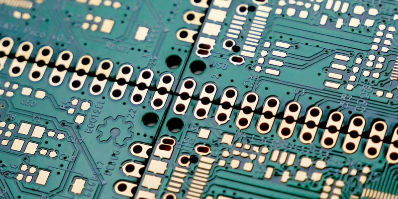
1 to 40 layers. Standard FR4 to Rogers high-frequency. HDI, rigid-flex, thick copper, and specialty substrates. Every board manufactured to IPC Class 2/3 standards with full traceability.
Our in-house PCB fabrication facility supports a full range of board types and specifications. All parameters below reflect standard production capability.
From standard FR4 multilayer to advanced HDI, rigid-flex, and specialty substrates. All fabricated in-house with full traceability.
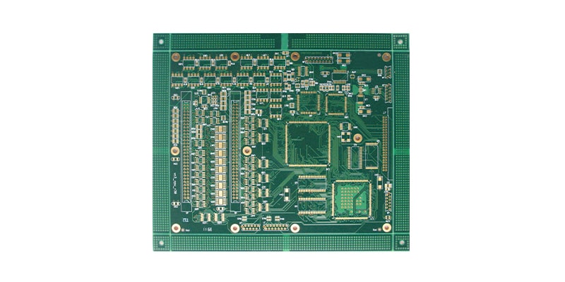
FR4 single, double, and multilayer PCBs. 1 to 40 layers, standard and high-Tg materials, suitable for most industrial and commercial applications.
High Density Interconnect PCBs with microvias, blind and buried vias, and fine-pitch traces for compact, high-performance designs.
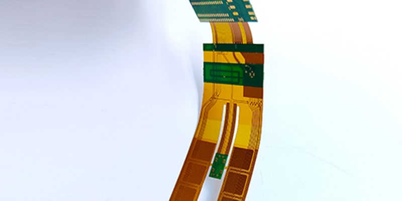
Combined rigid and flexible layers in a single board. Ideal for space-constrained applications requiring dynamic flex or 3D routing.
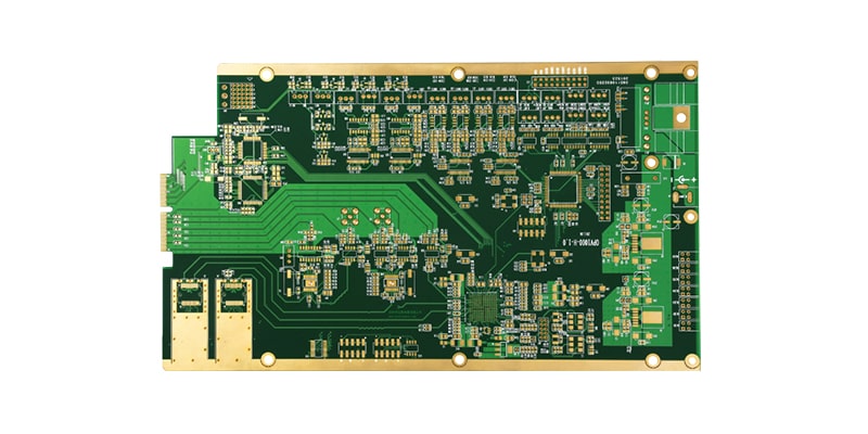
4 to 32 layer PCB fabrication with controlled impedance, tight registration, and consistent dielectric thickness across all layers.
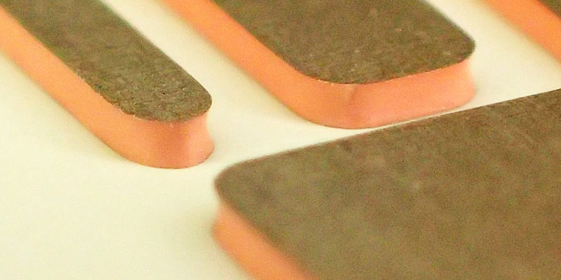
Heavy copper PCBs from 3.5oz to 10oz for power supply, automotive, and industrial applications requiring high current capacity.
Rogers, Isola, and PTFE-based substrates for RF, microwave, and high-speed digital applications requiring low loss and stable Dk.
Polyimide-based flexible PCBs for dynamic flex applications, wearables, and space-constrained assemblies requiring repeated bending.
Aluminum or copper base PCBs for LED lighting, power electronics, and applications requiring efficient heat dissipation.
Resin-filled and copper-capped via-in-pad technology for BGA and fine-pitch component placement on high-density boards.
Sequential lamination with blind and buried vias for HDI designs requiring layer-to-layer connections without through-board drilling.
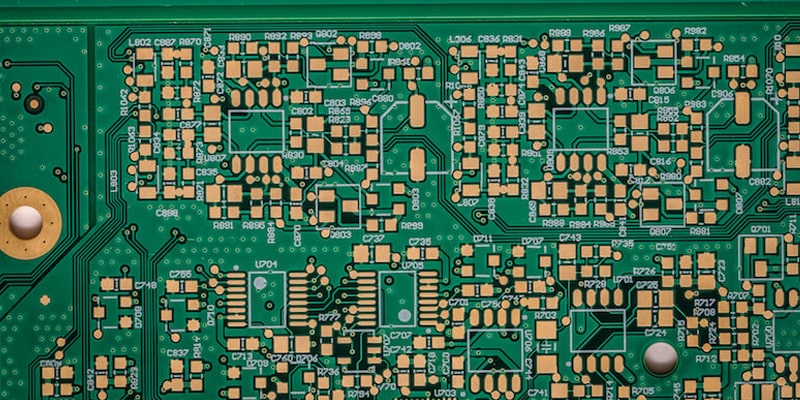
Controlled impedance PCBs for high-speed digital, RF, and microwave applications. Every board tested and certified before shipment.
PCB prototypes from 24 hours, MOQ 1 piece. DFM review included on every order before production begins.
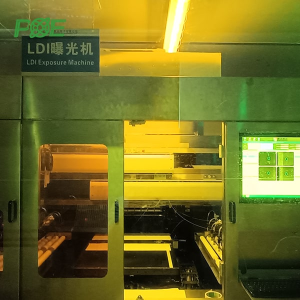
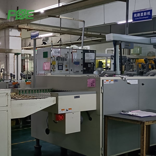
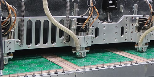
Click any step to see the equipment and process detail. Every board passes through the full sequence before leaving our facility.
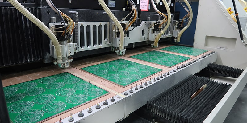
Premium FR4 substrate preparation and precision cutting. Material selection is the foundation of every high-quality PCB we source only certified laminates that meet IPC standards.
Every step of PCB fabrication from material cutting to final packaging is performed in our own facility. No outsourcing, no handoffs, full traceability on every board.
AOI, X-ray, flying probe, and electrical testing at every critical stage. 99.8% yield rate across all production runs, with full defect traceability.
ISO 9001, ISO 13485, ISO 14001, IPC-A-600, IPC-A-610, and IPC-6012 certified. Every board manufactured and inspected to IPC Class 2 or Class 3 as required.
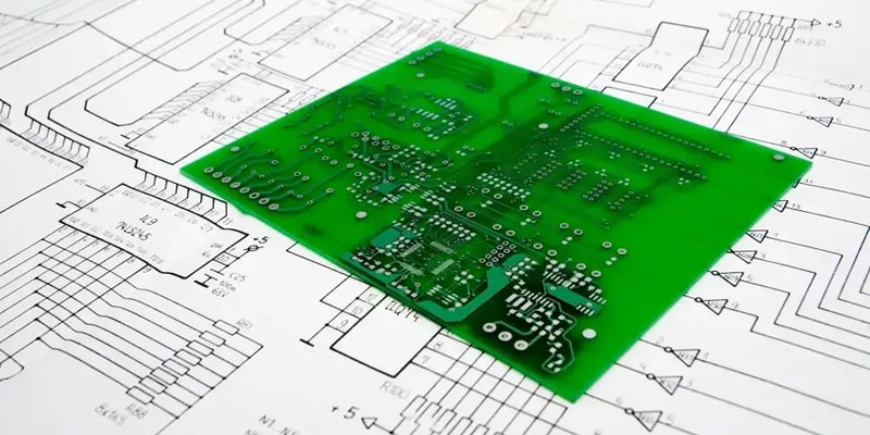
Every order receives a full DFM review before production begins. Our engineers flag issues that could affect yield, reliability, or assembly before they become problems.
Our facility and processes are certified to the most demanding international quality, environmental, and industry standards.
 ISO 9001:2015
 ISO 14001:2015
 ISO 13485:2016
 RoHS
RoHS REACH
REACH UL
UL IPC-A-610IPC-A-600IPC J-STD-001
 Email: all@poe-pcba.com
 Whatsapp: 85292069596
 Tel: 0755-25312250/ +8613798543496
 Factory Address: Floor 3, Jinyuan Industrial Park, No. 56, Tangtou Avenue, Shiyan Town, Baoan District, Shenzhen China


