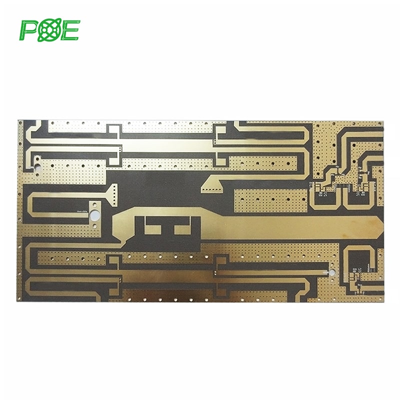
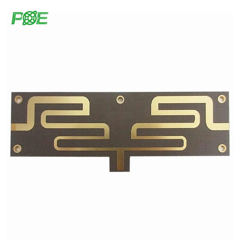
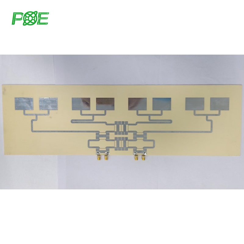
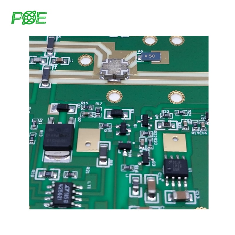
Layers
Single-sided, double-sided, and multilayer (up to 40+ layers)
Material
High-performance RF materials: Taconic, Rogers, Isola, PTFE, Arlon, and FR-4 High-Tg
DK (Dielectric Constant)
2.0 to 10.0 (±0.05 tolerance for high-frequency applications)
DF (Dissipation Factor)
Low values, typically <0.005 for high-frequency applications, with ±0.0005 tolerance
Board Thickness
0.1mm – 6.0mm (±0.05mm tolerance)
Copper Thickness
0.5 Oz (17.5 μm) – 5 Oz (175 μm)
Minimum Trace Width/Spacing
3mil/3mil (0.0762mm/0.0762mm) or better, depending on design and materials
Minimum Hole Size
0.15mm (6mil) – 0.4mm (16mil) or larger, depending on layer count
Operating Frequency
DC to 40GHz, optimized for RF/microwave applications
Maximum Board Size
500mm x 1100mm (20" x 44") or larger, varies with layer counts
Surface Finish
ENIG (preferred for RF), Immersion Silver, OSP, HASL, Lead-Free HASL
Solder Mask
Green, Blue, Yellow, Black, Red, White, and other colors
Solder Mask Resolution
3mil (0.0762mm) minimum
Solder Mask Registration
±2mil (±0.0508mm)
Silkscreen Color
White, Black, Yellow
Plated Through Holes (PTH)
Yes, with controlled aspect ratio up to 10:1
Blind & Buried Vias (BBV)
Yes, with precise depth control for impedance matching
Controlled Impedance
Yes, ±5% tolerance for critical RF traces (50Ω, 75Ω, 100Ω, etc.)
Electrical Testing
Continuity & isolation, impedance control, Hi-Pot, S-parameter testing for RF performance
Thermal Management
Advanced solutions including thermal vias, embedded heat sinks, and metal cores for high-power RF applications
RF Performance Testing
Network analyzer testing, insertion loss measurement, VSWR verification
Certification
ISO9001:2015, ISO13485:2016, ROHS, UL 94V0, IPC-600G Class II and IPC-6012B Class II standard

 Email: all@poe-pcba.com
 Whatsapp: 85292069596
 Tel: 0755-25312250/ +8613798543496
 Factory Address: Floor 3, Jinyuan Industrial Park, No. 56, Tangtou Avenue, Shiyan Town, Baoan District, Shenzhen China