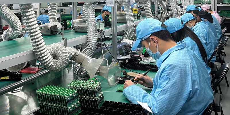
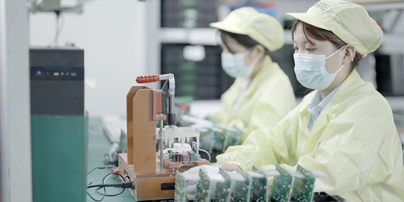
SMT, THT, and mixed-technology assembly from prototype to high-volume production. 4 high-speed SMT lines, 01005 to large BGA, IPC-A-610 Class 2/3 certified. Full turnkey with component sourcing, testing, and logistics.
Our in-house PCBA facility supports the full range of assembly types and component packages. All parameters reflect standard production capability.
From prototype to mass production, SMT to box build. All assembly performed in-house with full traceability and IPC-A-610 inspection.
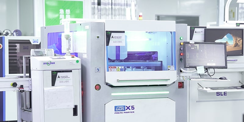
High-speed surface mount assembly on 4 automated SMT lines. 01005 to large BGAs, 0.25mm pitch, nitrogen reflow with 10-12 zone temperature control.
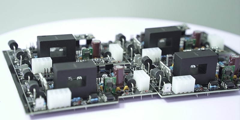
Through-hole and mixed-technology assembly. Wave soldering, selective soldering, and manual insertion for connectors, transformers, and large components.
Complete turnkey solutions including component sourcing, PCB fabrication, assembly, testing, and logistics. One supplier, full accountability.
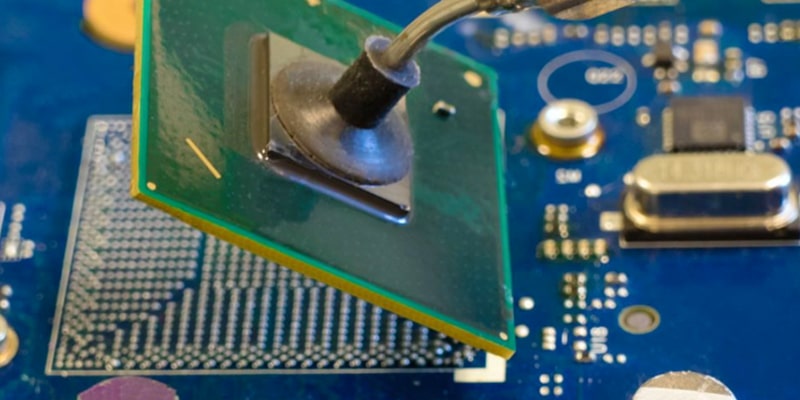
Fine-pitch BGA, micro-BGA, and CSP assembly with X-ray inspection. Minimum 0.25mm pitch, reflow profiling, and 100% X-ray verification.
PCB assembly prototypes from 24 hours, MOQ 1 piece. DFM and DFA review included. Ideal for engineering validation before committing to production.

Mass production assembly with cost optimization, dedicated line allocation, and statistical process control. Consistent quality at scale.
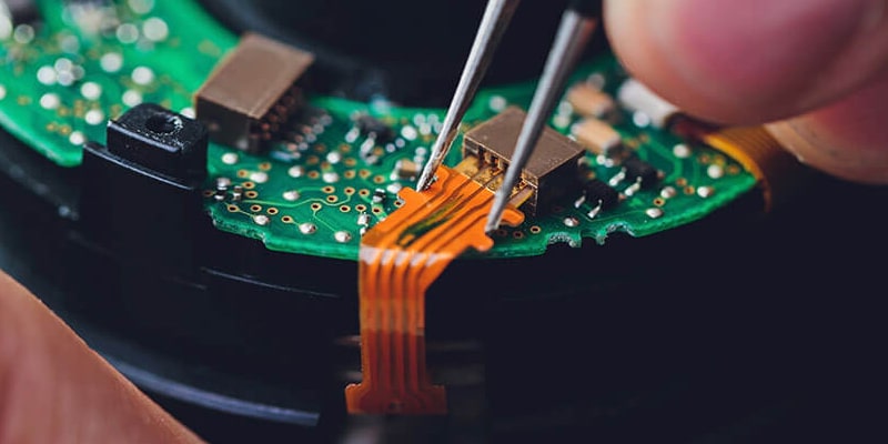
Specialized assembly for flexible and rigid-flex PCBs. Custom fixtures, controlled bend radius, and handling protocols for flex substrates.
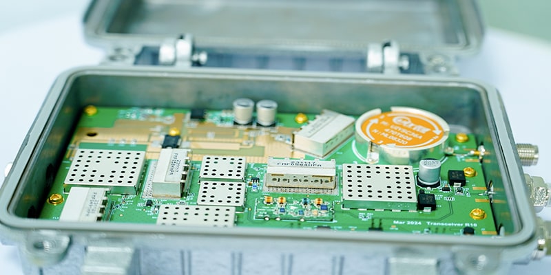
Complete system integration including enclosure assembly, cable harness, firmware programming, and functional testing. Ship-ready product.
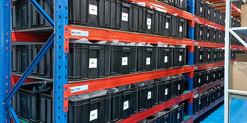
Global component procurement through authorized distributors. BOM review, alternative sourcing, and supply chain management for production continuity.
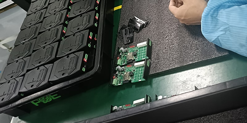
ICT, FCT, AOI, X-ray, and boundary scan testing. Every board verified against specification before shipment. Full test coverage documentation.
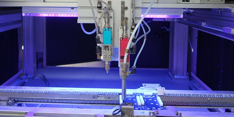
Selective and full-board conformal coating for harsh environment applications. Acrylic, silicone, and polyurethane coatings available.
Click any step to see the equipment and process detail. Every board passes through the full sequence before leaving our facility.
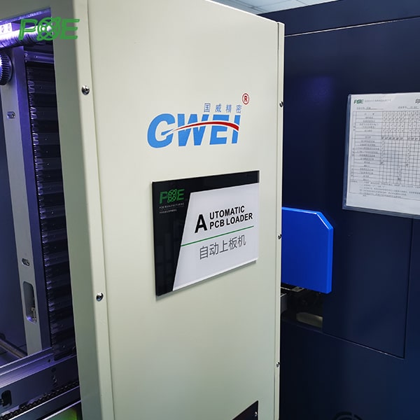
Seamless board feeding system that automatically loads PCBs onto the SMT line. Ensures consistent board positioning and eliminates manual handling errors at the start of production.
Every assembly inspected to IPC-A-610 Class 2 or Class 3 as required. Certified operators, documented processes, and full traceability on every board.
4 automated SMT production lines with 1M+ CPH capacity. 01005 to large BGA, 0.25mm pitch, nitrogen reflow with 10-12 zone temperature control.
Component sourcing, PCB fabrication, assembly, testing, and logistics under one roof. 35 dedicated procurement engineers and 10+ years of distributor relationships.
PCB assembly prototypes from 24 hours, MOQ 1 piece. DFM and DFA review included on every order before production begins.
Our assembly facility and processes are certified to the most demanding international quality, environmental, and industry standards.
 Email: all@poe-pcba.com
 Whatsapp: 85292069596
 Tel: 0755-25312250/ +8613798543496
 Factory Address: Floor 3, Jinyuan Industrial Park, No. 56, Tangtou Avenue, Shiyan Town, Baoan District, Shenzhen China