The 5 most common mistakes in PCB design
21 January 2025
Views: 1523
In the process of hardware circuit design, there are several errors that often occur. Let’s list five points.
1.Wiring error
Comparative differences between design and layout are major errors that cause the final stages of PCB design. So some things need to be double-checked.
Such as device size, via quality, pad size and review level, etc. In short, repeated confirmation checks need to be carried out against the design schematic diagram.
2.Pin error
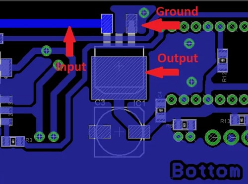
Series linear regulated power supplies are cheaper than switching power supplies, but their power conversion efficiency is low. Typically, many engineers choose to use linear regulated power supplies due to their ease of use and low price. But it should be noted that although it is very convenient to use, it will consume a lot of power and cause a lot of heat to spread. In contrast, switching power supplies are more complex in design but more efficient. However, everyone needs to pay attention to the fact that the output pins of some regulated power supplies may be incompatible with each other, so you need to confirm the relevant pin definitions in the chip manual before wiring.
3.Lead width
When the current of the PCB leads exceeds 500mA, the first wire diameter of the PCB will appear to be insufficient in capacity. For a typical thickness and width, wires on the surface of a PCB can pass more current than wires inside a multilayer circuit board because surface leads can diffuse heat through air flow.
The width of the line is also related to the thickness of the copper foil of the layer. Most PCB manufacturers allow you to choose from different thicknesses of copper foil from 0.5 oz/sq.ft to 2.5 oz/sq.ft.
4.Tombstone device
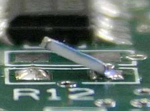
When using the reflow process to solder some small surface-mount devices, the device will form a single-end warping phenomenon under the infiltration of solder, commonly known as "tombstone".
This phenomenon is usually caused by asymmetric wiring patterns, which cause uneven heat diffusion on the device pads. Tombstone occurrence can be effectively mitigated using the correct DFM inspection.
5.Corrosion trap
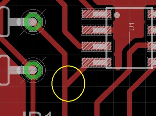
Corrosion traps may form when the angle between PCB leads is too small.
These sharp-angled connections may have residual corrosive liquid during the corrosion stage of the circuit board, which will remove more copper there, thus forming stuck points or traps.
Later, it may cause the lead to break and form an open circuit. Due to the use of photosensitive etching solutions in modern manufacturing processes, this corrosion trap phenomenon has been greatly reduced.
Share This Story, Choose Your Platform!

 Email: all@poe-pcba.com
 Whatsapp: 85292069596
 Tel: 0755-25312250/ +8613798543496
 Factory Address: Floor 3, Jinyuan Industrial Park, No. 56, Tangtou Avenue, Shiyan Town, Baoan District, Shenzhen China


