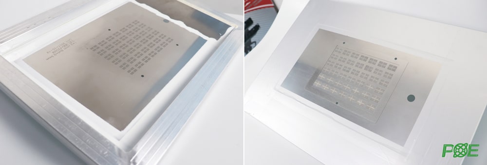
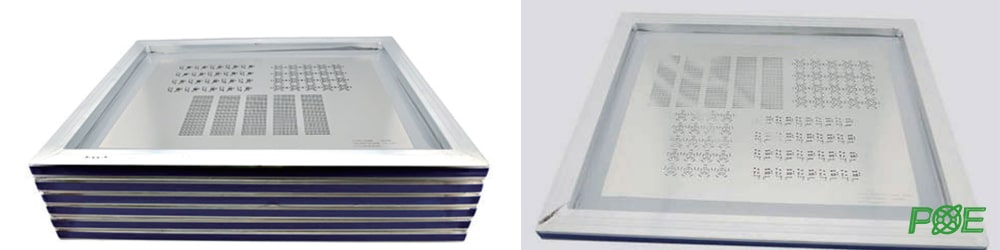
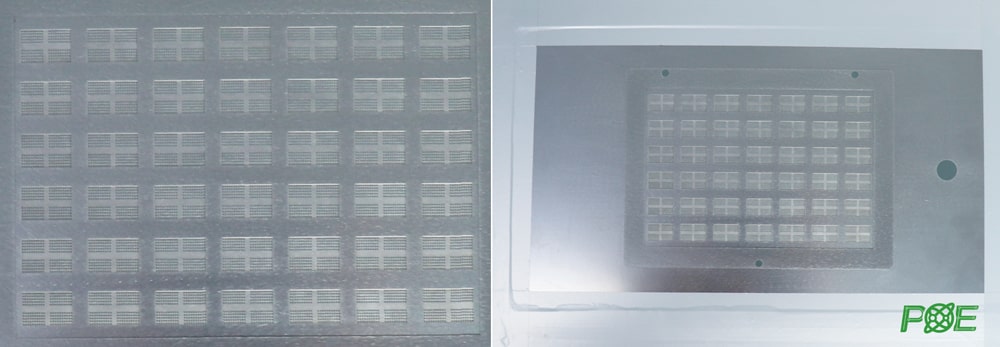
SMT Stencil
1.What is stencil?
The purpose of an SMT stencil is to transfer solder paste to a bare PCB. A stainless steel foil is laser cut creating an opening for every surface mount device on the board. Once the stencil is properly aligned on top of the board, solder paste is applied over the openings. When the stainless steel foil is separated from the board, solder paste will remain, and the board is ready for placement of the SMD.
2.Material: INOX stainless steel SUS304
3.Mainly used Stencil Type:
(1) Laser cut SMT stencil, most common paste stencil type nowdays;
(2) Electroformed stencil, offer the best paste release characteristics and frequently used for fine pitch SMT applications such as BGA;
(3) Step stencil, with two or more different stencil thickness in a same steel plate, because different components have paste requirement;
(4) Nano Coated Stencils, very high precision of the opening position, Smart SMT Tools has leveraged its chemistry knowledge to develop unique nano coatings that improve various steps in the PCB Assembly process.
4.Regular size
5.How to choose the suitable thickness of SMT stencils?
Solder paste process
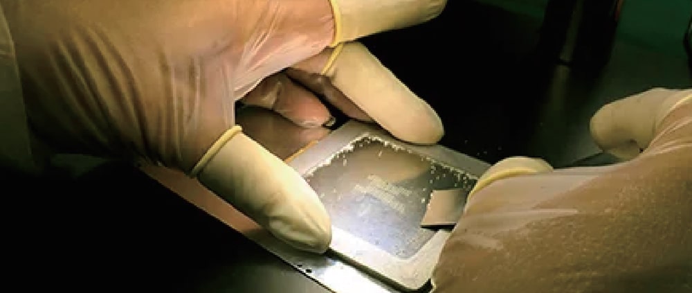
6.How to inspect the quality of stencil:
(1) Size of the frame meets the requirements, the quality of taut mesh, the tauter, the better quality of printing;
(2) Check the appearance quality of the template mesh for obvious defects, such as the shape of the mesh, high density or narrow spacing of the pins adjacent to each other with no abnormalities;
(3) Use a magnifying glass or microscope to check whether the flare of the pad opening is downward, whether the inner wall around the opening is smooth, withd or without burrs, focusing on checking the processing quality of the narrow-pitch IC pin opening;
(4) The product's printed board is placed on the bottom surface under the template, and the leakage holes of the template are used to align the printed board pad graphics, checking that the graphics are perfectly aligned, and that there are no multiple holes (unwanted openings) and fewer holes (missed openings).
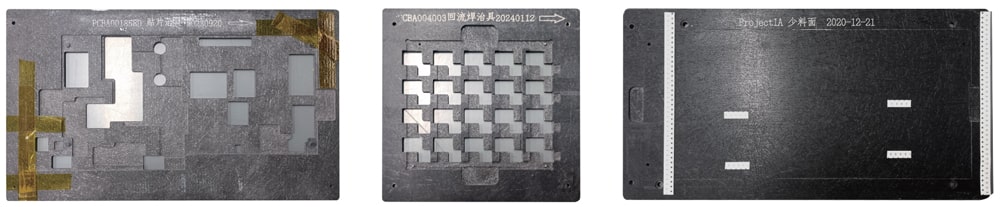
Tray for wave oven
Tray, a tooling fixture to protect the PCB and components during wave soldering process, avoid PCB deformation, and assist in supporting and positioning. Which is suitable for PTH components.
What is the function of wave soldering tray?
The main points are as follows:
1. Solve the bad phenomena such as component floating height, skew, and insufficient tin.
2. Prevent overflow tin from contaminating the PCB and prevent PCB bending and deformation.
3. Irregular-shaped PCB must use the tray when via the wave soldering oven.
4. Avoid contamination of golden fingers.
What kind of PCB designs require the use of wave soldering trays/fixtures?
(1) Double-sided PCB Assembly: Especially when one side of the PCB has been completed SMT soldering, and the other side needs to be through the wave soldering to solder through-hole components (such as DIP packages), the use of fixtures can effectively protect the side that has already been soldered from damage, and to ensure that the components on the soldered side are properly aligned and supported;
(2) Large or Heavy Components: For PCBs with large or heavy components mounted on them, the use of fixtures prevents components from shifting or falling off due to their own weight or vibration during the soldering process;
(3) Sensitive Component Protection: PCB design containing sensitive components (such as fragile ceramic capacitors, crystal oscillators, etc.), fixtures can be designed with a specific protection structure to avoid thermal shock or physical damage to these components during the soldering process;
(4) Improve Productivity and Yield: In a mass production environment, fixtures ensure consistency and accuracy of soldering, reducing human error and improving productivity and product quality;
(5) Special Shapes or Sizes of PCBs: Non-standard shapes or sizes of PCBs may be difficult to pass directly through the wave soldering machine, and fixtures can be adapted to ensure that these PCBs pass smoothly through the soldering process;
(6) Reduce or Avoid PCB Deformation: Larger PCBs are particularly susceptible to deformation during heating and cooling cycles. Fixtures help reduce this deformation by evenly distributing pressure and providing additional support.
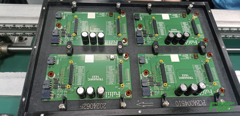
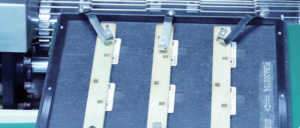
Tray for Reflow oven
Fixture used in the current reflow soldering process, Reflow soldering is suitable for SMD electronic components
The bending deformation problem of the printed circuit board (PCB) is often encountered. This is due to the fact that the PCB board is subjected to gravity when it is heated. The function of the reflow soldering fixture is to fix the PCB board in it and prevent the board from deforming during the soldering process.
(1) Prevent Deformation and Warping: For large-area, thin or long PCBs, the reflow process may cause deformation or warping due to thermal stress, the use of trays can provide uniform support, reduce deformation, and ensure the flatness of the PCB during the heating and cooling process;
(2) Mass Production: In mass production, the use of standardized reflow trays increases productivity, reduces manual handling, and ensures consistency and repeatability of the reflow process every time;
(3) Protecting Sensitive Components: For PCBs that have been preloaded with fragile or heat sensitive components, the tray can be designed with a shielding or heat dissipation structure to protect these components from excessive temperatures and avoid damage;
(4) Special Process Requirements: When a PCB design contains specific areas that require special handling, such as localized needs for higher or lower reflow temperatures, the tray can be designed with special materials or structures to help achieve these process requirements;
(5) FPC: For flexible PCBs, reflow trays provide the necessary support and protection against unwanted bending or damage during the heating process, while maintaining their stability during transport.
Bed-of-Nails Test Fixture
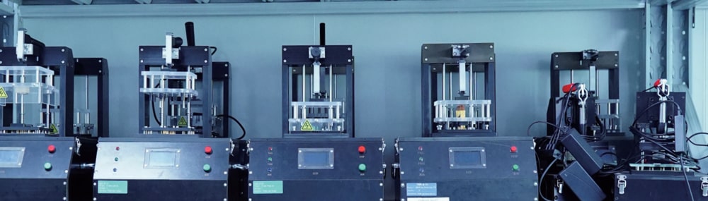
Function Testing Jig, they are custom made according to the size of the PCBA board, the location of the test point, and the value. Acrylic, plastic, metal probes, display screens, wires, and simple PCB circuit boards are mainly used to complete the entire test fixture production. Function test is one of QC process which can 99.9% ensure quality of PCBA manufactured. Test JIG Purpose Test JIGs are used for functional testing and quality inspection of PCBA products, ensuring that each board is rigorously verified for performance before shipping. High-quality test JIGs improve test efficiency and accuracy.
Test the JIG production process
1.Design: Design the test JIG according to the product test requirements, determine the test points and test methods;
2.Material Selection: Select suitable material (e.g. Bakelite, aluminum alloy) to make JIG;
3.Processing: Adopt CNC and other processing technology to make JIG;
4.Testing & Calibration: Verifying the alignment of the probe/Checking the connectivity of the interface/Verifying the control electronics;
5.Quality Inspection: Strict quality inspection is required to ensure that its quality and performance meet customer requirements. During the testing process, some issues may be discovered that require corresponding repairs and adjustments;
6.Management Standards: In the production process of PCBA testing fixtures, certain management standards need to be followed, including the R&D department providing relevant product information, the engineering department evaluating the production requirements of testing fixtures and conducting acceptance and maintenance;
7.Leadtime Cycle: Generally 2-3days, or 2-3 weeks. Lead time of PCBA testing fixtures varies depending on the complexity of the fixture and production requirements.
Advantages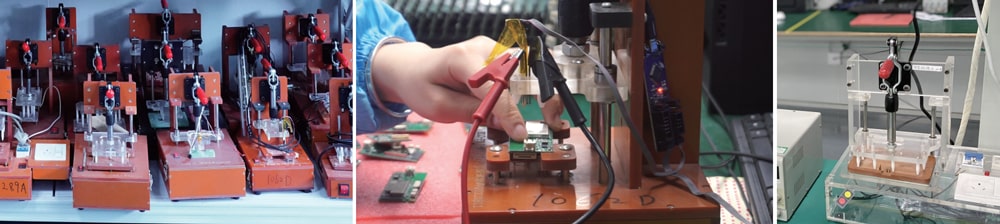 POE enables you to speed up development by providing PCBA (PCB assembly) test fixture designs in a single day. There are always two main applications for test fixtures, one is firmware upload and the other is functional testing. PCBA functional tests can be developed earlier and shorter by reducing the time required to design productive fixtures.
Supported formats:
Altium (.csv) / Eagle (.brd) / Gerbers (.zip) / KiCAD (.kicad_pcb).
The larger the test probe, the more durable it is, and the larger the probe, the cheaper it is. At POE we use 100 mil (2.54mm) and 75 mil (1.91mm) spacing.
What do we need to prepare testing JIG?
(1) PCB Design File: Including Gerber and CAD drawing, it shows layout and dimensions of the PCB and help pinpoint test points;
(2) Test Point List: List all the Net names, location coordinates, and test types (e.g., open/short test, electrical performance test, etc.) to ensure that the probes on the test fixture can accurately contact the test points.
(3) Component Position and Height: Also we can use first Article of assembled PCBA to measure and get the figure;
(4) Test Specification: Define the test criteria for each test point, including electrical parameters such as voltage, current, resistance, frequency, etc., as well as test conditions and pass/fail criteria;
(5) Functional Test Requirements: Detailed description of the functional test items that need to be performed, such as power supply test, signal integrity test, software interaction test and so on;
(6) Interface Information: If the test fixture needs to be connected to an external test instrument or computer, it is necessary to provide the relevant interface type (such as USB, Ethernet, GPIB, etc.) and communication protocol information;
(7) Special Requirements: Such as electrostatic protection requirements, ease of operation requirements, automation needs, etc., which will affect the design of the jig and material selection.

 Email: all@poe-pcba.com
 Whatsapp: 85292069596
 Tel: 0755-25312250/ +8613798543496
 Factory Address: Floor 3, Jinyuan Industrial Park, No. 56, Tangtou Avenue, Shiyan Town, Baoan District, Shenzhen China


