Printed Circuit Board Assembly: A Step-by-Step Ultimate Guide
21 January 2025
Views: 10850
In today's technology-driven world, printed circuit boards are the backbone of electronic devices. The process of printed circuit board assembly involves connecting components to create functional circuits, and understanding each step of the PCB assembly process is crucial. This ultimate step-by-step guide will walk you through every aspect of PCB assembly.

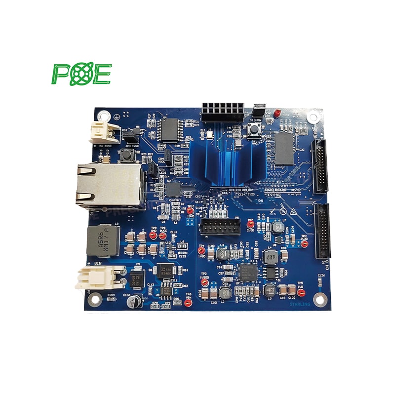
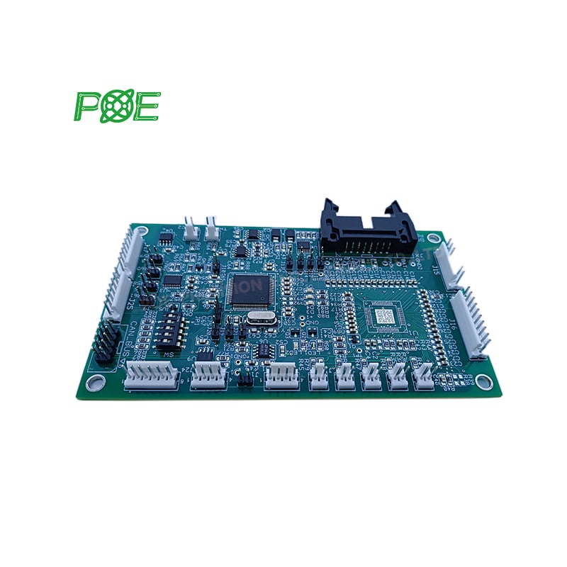
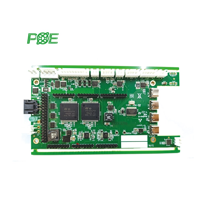
Printed circuit board assembly steps
1.PCB Design
The first step in PCB assembly is creating the design, specialized computer-aided design (CAD) software is typically used to design schematics and layouts, ensuring correct component placement and connections, while adhering to design rules, defining trace widths, layer stack-up, and component footprint space is also crucial at this stage.

2.Gerber File Generation and Review
After completing the design, export Gerber files containing important information about PCB layers and copper patterns to ensure accurate manufacturing. You can also send Gerber files to our POE printed circuit board assembly manufacturer for review and verification.

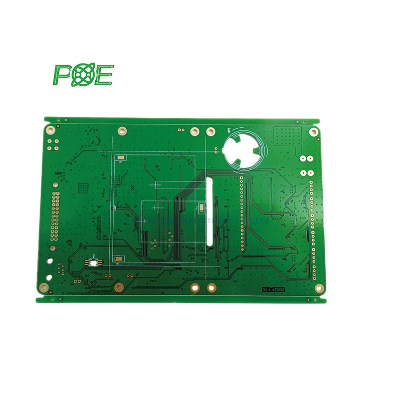
3.PCB Manufacturing
Turning the design into a PCB involves various processes such as: 1. Selecting substrate and copper-clad laminates; 2. Applying photoresist and photomasks; 3. Etching to create traces; 4. Drilling for through-hole components and vias; 5. Plating and chemical deposition; 6. Applying solder mask and silk screen. After these processes, you'll have a finished standard PCB.

4.Material Procurement
Purchase electronic components needed for your PCB project based on your requirements, Ensure that the components are of high quality and purchased from reliable suppliers, A well-organized bill of materials (BOM) is crucial at this stage.

5.Component Preparation
Two common methods for organizing and preparing electronic components for PCB assembly are: 1. Surface-mount technology (SMT); 2. Through-hole technology (THT).
6.PCB Loading
The first step in SMT is the loading machine, which pushes the printed circuit board into line with the solder paste printer.
7.Stencil Production
Create a template to accurately apply solder paste to surface-mount components on the PCB.
8.Solder Paste Application
Align the template with the PCB and use a rubber squeegee to apply solder paste to the pads. Be careful to apply the correct amount of solder paste to avoid defects.

9.Component Placement
Place components in the designated positions according to the CAD layout. High-precision pick-and-place machines are typically used for automated PCB assembly processes.

10.Soldering
Depending on the PCB assembly technology, the following methods can be used to solder components:
Reflow Soldering (SMT): The PCB is placed in a reflow oven to melt the solder paste, creating connections between the components and the circuit board.

Wave Soldering (THT): The PCB is passed through a molten solder wave, adhering to exposed pads and component leads.

Manual Soldering (THT): Skilled technicians use a soldering iron to manually solder the components in place.
11.Post-Solder Inspection
Use automated optical inspection (AOI), X-ray inspection, or manual inspection by experienced technicians to check the quality of PCB soldering.

12.Testing and Debugging
Various techniques, such as online testing, flying probe testing, and functional testing, are used to test the functionality of the assembled PCB.

13.Final Assembly and Packaging
Connect all necessary connectors, heat sinks, enclosures, and other hardware, and package the complete PCB assembly for shipping.

Conclusion
By following this ultimate step-by-step guide to PCB assembly, you can ensure that the final product is fully functional and efficient. Understanding the complexity of this process will help you create high-quality electronic devices, paving the way for success in your projects and innovations. POE has over 20 years of PCB assembly experience, specializing in providing customers with one-stop PCB assembly services. If you need more information, please feel free to contact us for professional advice.


 Email: all@poe-pcba.com
 Whatsapp: 85292069596
 Tel: 0755-25312250/ +8613798543496
 Factory Address: Floor 3, Jinyuan Industrial Park, No. 56, Tangtou Avenue, Shiyan Town, Baoan District, Shenzhen China