Printed Circuit Boards are the fundamental components used in almost all electronic devices today. PCBs come in different layers, typically ranging from 1 to 40 layers. The more layers a PCB has, the better its functionality, reduced space requirements, and improved performance. With the increasing complexity of electronic technology and the constant development of more compact and faster electronic devices, the demand for advanced PCB solutions continues to grow, making multilayer PCBs the preferred choice.

What is a Multilayer PCB?
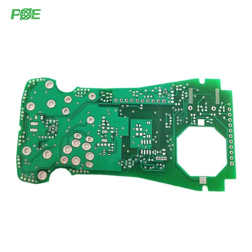
A multilayer PCB is a type of printed circuit board composed of multiple layers of conductive materials sandwiched together. Unlike single-layer PCBs where components are located on one side of the board, multilayer PCBs have components and electrical connections on both sides, allowing for more complex and compact circuitry. The layers of the circuit board are separated by insulation layers, and the connections between the layers are made through small holes or vias drilled on the PCB. These layers are stacked and laminated together to form a single unified board. The number of layers can range from two to over forty, with each layer serving a specific purpose, such as power layers, ground layers, or signal routing layers. Multilayer designs enable greater interconnectivity between components, making them an ideal choice for high-density applications.
Common PCB Layer Configurations:
Single-layer PCB: A single-layer PCB has only one conductive layer made of copper laminated onto a non-conductive substrate. Components and connections exist on one side of the circuit board, limiting the complexity of routing. It is typically used in simple electronic devices, low-cost consumer products, basic power supplies, and timing circuits.
Double-layer PCB: Double-layer or double-sided PCBs consist of two conductive layers, allowing for components and electrical connections on both sides of the circuit board. Compared to single-layer PCBs, they offer increased routing complexity. They are commonly used in consumer electronics (such as amplifiers, power supplies, LED lighting systems), industrial control and instrumentation, automotive electronics, and more.
4-layer PCB: A 4-layer PCB consists of four conductive layers separated by insulating materials. It includes two inner layers (power and ground layers) and two outer layers for component placement and signal routing. Using inner layers simplifies routing and reduces signal interference, enabling more complex circuit designs. They are typically used in advanced consumer electronics (such as smartphones, laptops), telecommunications equipment, high-density electronic devices, and more.
8-layer PCB: An 8-layer PCB has eight conductive layers, providing a higher level of complexity for electronic circuits. It allows for higher-density routing and performs better in terms of signal integrity and noise reduction, making it suitable for high-speed and high-frequency applications. They are commonly used in complex communication systems, medical devices, high-performance computing, servers, and more.
PCBs with more than 8 layers: PCBs with more layers, reaching up to 40 layers or more in special cases, offer the highest level of complexity and are used in applications requiring high-density circuits and optimal performance. They are typically used in aerospace and defense electronics, satellite systems, high-speed computer networks and data centers, advanced imaging and sensing systems.
Advantages of Multilayer PCBs
Based on the above introduction, the advantages of multilayer PCBs are as follows:
High Density: Multilayer PCBs allow for more compact devices without compromising performance. They accommodate a large number of components in a smaller area, making them an ideal choice for devices like smartphones and laptops.
Signal Integrity: Multilayer boards improve signal integrity by incorporating additional ground layers, reducing electromagnetic interference (EMI), and providing stable voltage reference levels.
Better Heat Management: The multiple layers in a multilayer PCB facilitate heat distribution throughout the board, reducing thermal stress and improving overall device performance.
Enhanced Design Flexibility: These boards provide enhanced design options for complex electronic circuits, allowing for the integration of high-speed circuits, flexible circuits, and high-frequency components.

Multilayer PCB Manufacturing Process
Having understood the advantages and common applications of multilayer PCBs, let's take a look at the manufacturing process:
Material Selection: Choosing the right materials for the substrate, conductive layers, and laminates is crucial for achieving optimal PCB performance. Typical materials include FR-4 glass fiber epoxy resin for the substrate and copper for the conductive layers.
Circuit Design and Layer Stacking: Engineers use computer-aided design software to design the circuit layout. The optimal number of layers is determined based on factors such as signal integrity, power requirements, and space constraints.
Layer Separation and Lamination: Individual layers are manufactured separately and then laminated together. Special adhesive sheets with pre-impregnated resin are used to apply heat and pressure to bond the layers.
Drilling, Plating, and Imaging: Precision drilling creates necessary alignment and interconnections between the layers. These drilled holes, called vias, are then plated with a conductive material to establish electrical connections. The layers are then imaged with a photoresist and exposed to UV light to define the circuit patterns.
Copper Etching: The exposed copper is etched away using a chemical process, leaving behind the desired copper traces and pads for component placement.
Soldermask and Silkscreen Printing: A soldermask layer is applied to protect the copper traces and pads while leaving the component mounting areas exposed. Silkscreen printing is used to add labels, component designators, and other markings on the PCB.
Surface Finish: A surface finish is applied to protect the exposed copper surfaces from oxidation and facilitate soldering during component assembly. Common surface finishes include HASL (Hot Air Solder Leveling), ENIG (Electroless Nickel Immersion Gold), and OSP (Organic Solderability Preservative).
Testing and Inspection: The completed multilayer PCB undergoes various testing and inspection processes to ensure its functionality, electrical connectivity, and quality. These tests may include automated optical inspection (AOI), electrical testing, and functional testing.
Component Assembly: Once the PCB passes all the tests, electronic components such as resistors, capacitors, integrated circuits, and connectors are soldered onto the board using automated assembly equipment or manual soldering techniques.
Final Testing: The assembled PCB undergoes final testing to verify its functionality and performance. This may include functional testing, environmental testing, and reliability testing.
Conclusion
Multilayer PCBs offer numerous advantages over single-layer and double-layer PCBs, making them essential for modern electronic devices. They provide higher density, improved signal integrity, better heat management, and enhanced design flexibility.With their ability to accommodate complex circuitry and compact designs, multilayer PCBs play a crucial role in advancing electronic technology across various industries.If you have PCB manufacturing and assembly needs, please feel free to contact us POE. We have more than 20 years of experience in PCB manufacturing and assembly, and can manufacture 100% reliable 1-40 layer PCBs. Contact us to learn more!

 Email: all@poe-pcba.com
 Whatsapp: 85292069596
 Tel: 0755-25312250/ +8613798543496
 Factory Address: Floor 3, Jinyuan Industrial Park, No. 56, Tangtou Avenue, Shiyan Town, Baoan District, Shenzhen China