| Shape | Illustrate |
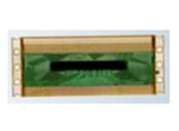 |
COF (Chip On Flex, or Chip On Film, often called Chip On Film) is a soft film construction technology that fixes ICs on flexible circuit boards. It uses soft additional circuit boards as packaging chip carriers to connect the chips to the flexible substrate. Technology of circuit joining. |
| COF | |
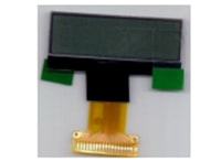 |
The size of a COG (Chip on glass) LCD module is easy to mass produce, and is used in consumer electronics, such as mobile phones, PDAs, etc. That is, the chip is directly bound to the glass. This method can greatly reduce the overall |
| COG | |
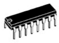 |
DIP (dual in-line package) dual in-line package. One of the plug-in packages, the pins are drawn from both sides of the package. The packaging materials include plastic and ceramic. DIP is the most popular plug-in package, and its application range includes standard logic IC, memory LSI, microcomputer circuits, etc. The pin center distance is 2.54mm, and the number of pins is from 6 to 64. Package width is typically 15.2mm. Some packages with widths of 7.52mm and 10.16mm are called skinny DIP and slim DIP (narrow DIP) respectively. But in most cases, no distinction is made and they are simply referred to as DIP. In addition, ceramic DIP sealed with low melting point glass is also called cerdip. |
| DIP | |
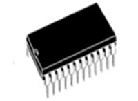 |
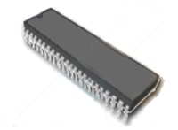
PDIPP-plasti, a symbol indicating plastic packaging. For example, PDIP means plastic DIP. |
| PDIP | |
 |
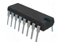
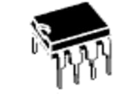
SDIP (shrink dual in-line package) center distance (1.778mm) is smaller than DIP (2.54mm), hence the name. Pin count ranges from 14 to 90. There is also one called SH-DIP. There are two types of materials: ceramic and plastic. |
| SDIP | |
 |
Shrinkable DIP. One of the plug-in packages, the shape is the same as DIP, but the pins are SKDIP/SKY (Skinny Dual In-line Packages) narrow body DIP. Usually collectively referred to as DIP (see DIP). A type of DIP. Refers to the width of 7.62mm and the pin center distance of 2.54mm |
| SKDIP/SKY | |
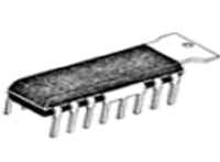 |
A type of DIP. |
| DIP-tab | |
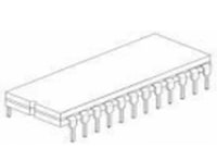 |
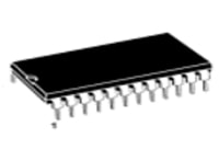
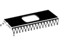
CDIPC-ceramic, the symbol for ceramic packaging. For example, CDIP represents ceramic DIP, which is a symbol often used in practice. |
| CDIP | |
 |
NO |
| PCDIP | |
 |
NO |
| FDIP | |
 |
NO |
| PSDIP | |
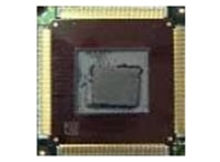 |
DICP (dualtape carrier package) double-sided pin load package. One of TCP (load encapsulation). The pins are made on insulating tape and lead out from both sides of the package. Due to the use of TAB (automatic load soldering) technology, the package appearance is very thin. It is often used in LCD driver LSI, but most of them are customized products. In addition, the 0.5mm thick memory Ls1 book-shaped package is in the development stage. In Japan, DICP is named DTP in accordance with the standards of the EIAJ (Electronic Machinery Industry of Japan) Association. |
| DICP | |
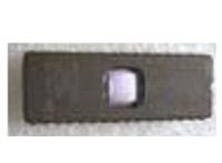 |
Another name for ceramic DIP (including glass seal). |
| DIC | |
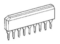 |
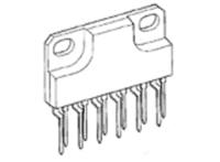
DIC (dualin-lineceramicpackage) SIP (single in-line package) single in-line package. The pins are led out from one side of the package and arranged in a straight line. The package stands on its side when assembled to a printed circuit board. The pin center distance is usually 2.54mm, and the number of pins ranges from 2 to 23. Most of them are customized products. Packages come in various shapes. Some also call packages that have the same shape as ZIP as SIP. |
| SIP | |
 |
NO |
| ZIP/EZIP | |
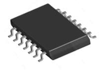 |
SOP (Small Outline Packages) small outline pin packages. |
| SOP | |
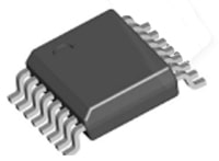 |
SSOP (Shrink Small-Outline Package) is a small outline package (SOP). Narrow pitch and small appearance plastic package, developed by Philips in 1968~1969 |
| SSOP | |
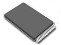 |
TSOP (Thin Small Outline Package) means thin small size package. TSOP memory has pins made around the chip and is directly attached to the surface of the PCB board using SMT technology (surface mounting technology). |
| TSOP | |
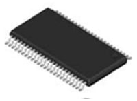 |
TSSOP (Thin Shrink Small Outline Package) is a thin shrink-type SOP. It is thinner than SOP, has denser pins, and has a smaller package size for the same function. |
| TSSOP | |
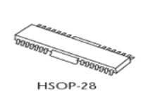 |
HSOP (Head Sink Small Outline Packages)H-(with heat sink), indicating the mark with radiator. For example, HSOP means SOP with heat sink. |
| HSOP | |
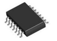 |
DFP (dual flat package) double-sided pin flat package. Is another name for SOP (see SOP). This term used to be used in the past, but it is basically no longer used. DIC (dual in-line ceramic package) is another name for ceramic DIP (including glass seal) (see DIP). |
| DFP | |
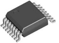 |
DSO (dual small out-lint) double-sided pin small outline package. Another name for SOP (see SOP). Some semiconductor manufacturers use this name. |
| DSO | |
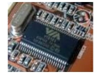 |
MFP (mini flat package) small flat package. Another name for plastic SOP or SSOP (see SOP and SSOP). A name adopted by some semiconductor manufacturers. |
| MFP | |
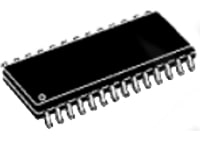 |
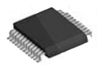
SO (small out-line) Another name for SOP. Many semiconductor manufacturers in the world use this nickname. |
| SO | |
 |
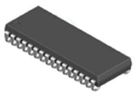
SOIC (small out-line integrated circuit) Another name for SOP (see SOP). Many foreign semiconductor manufacturers use this name |
| SOIC | |
 |
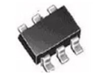
SOJ (Small Out-Line J-Leaded Package) J-shaped pin small outer package. One of the surface mount packages. The pins are drawn downward from both sides of the package in a J-shape, hence the name. Usually plastic products, most of them are used in memory LSI circuits such as DRAM and SRAM, but most of them are DRAM. Many DRAM devices packaged in SOJ are assembled on SIMMs. The pin center distance is 1.27mm, and the number of pins is from 20 to 40 (see SIMM) |
| SOJ | |
 |
SOT (Small Outline Transistor) is a small outer transistor, a type of SOP series package. |
| SOT | |
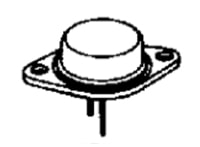 |
TO (Transistor Outline) transistor packaging. |
| TO3 | |
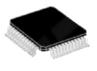 |
QFP (quad flat package) four-side pin flat package. One of the surface mount packages, the pins are drawn out from four sides in a gull wing (L) shape. There are three types of base materials: ceramic, metal and plastic. In terms of quantity, plastic packaging accounts for the vast majority. When the material is not specifically shown, in most cases it is plastic QFP. Plastic QFP is the most popular multi-pin LSI package. Not only used in digital logic LSI circuits such as microprocessors and gate arrays, but also in analog Ls1 circuits such as VTR signal processing and audio signal processing. The pin center distance has various specifications such as 1.0mm, 0.8mm, 0.65mm, 0.5mm, 0.4mm, 0.3mm, etc. The maximum number of pins in the 0.65mm center distance specification is 304. Japan calls QFP with pin center distance less than 0.65mm QFP (FP). But now the Japan Electronics Machinery Industry Association has re-evaluated the form factor of QFP. There is no distinction in the pin center distance, but according to the thickness of the package body, it is divided into three types: QFP (2.0mm~3.6mm thick), LQFP (1.4mm thick) and TQFP (1.0mm thick). In addition, some Lsi manufacturers specifically call QFP with a pin center distance of 0.5mm as shrinkable QFP or SQFP or VQFP. However, some manufacturers also call QFP with pin center distances of 0.65mm and 0.4mm as SQFP, which makes the name a little confusing. The disadvantage of QFP is that when the pin center distance is less than 0.65mm, the pins are easy to bend. In order to prevent pin deformation, several improved QFP varieties have appeared. For example, BQFP with tree finger cushions at the four corners of the package (see BQFP); GQFP with a resin protective ring covering the front of the pin (see GQFP); test bumps are set in the package body and placed to prevent lead deformation. TPQFP that can be tested in a special fixture (see TPQFP). In terms of logic LSI, many development products and high-reliability products are packaged in multi-layer ceramic QFP. Products with a minimum pin center distance of 0.4mm and a maximum pin count of 348 are also available. In addition, there are also ceramic QFPs sealed with glass. |
| QFP | |
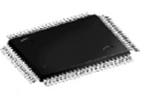 |
LQFP (low profile quad flat package) thin QFP. Refers to QFP with a package body thickness of 1.4mm. It is the name used by the Japan Electronics Machinery Industry Association based on the new QFP form factor. |
| LQFP |