How to choose Heavy copper PCB?
21 January 2025
Views: 1281
Heavy copper PCB is widely used in electronics, automobiles, industry and other fields. Different thick copper PCBs have different requirements for different fields. Let us understand the related issues of heavy copper PCB.

1. What is heavy copper PCB?
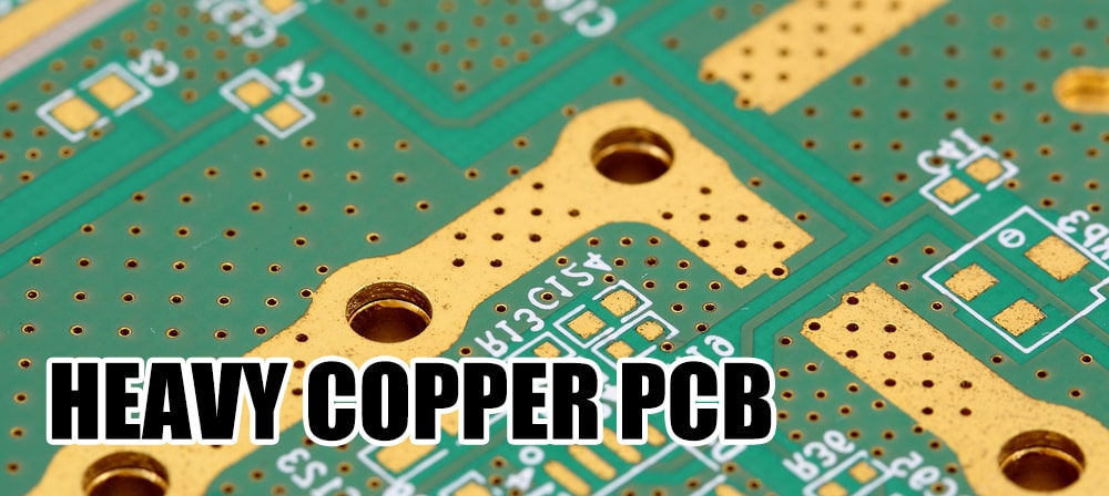
Heavy copper PCB is a layer of copper foil bonded to the outer layer of the circuit board. When the copper thickness is greater than 2oz, it is defined as heavy copper PCB. The thickness of copper is different, and the applicable scenarios are also different.
2. What are the advantages of heavy copper PCB?
heavy copper PCB is more resistant to high temperatures, low temperatures, and corrosion. More importantly, it can carry higher currents and avoid excessive heating, allowing the product to have a longer service life. Thick copper plates have a wide range of applications. heavy copper PCB may be used in various common home appliances, high-tech products, military, medical and other equipment.
3. Standards for heavy copper PCB
PCB copper thickness is generally divided into 1oz (35um), 2oz (70um), 3oz (105um), and can also be made thicker. For applications that need to withstand high currents, such as power supplies with larger currents, 2oz is generally used. For high-frequency products that need to transmit high-frequency signals, the common ones are 1oz or even smaller, reducing the copper thickness to reduce signal transmission losses. In addition, 1oz of common ordinary circuit boards is enough.
4.heavy copper PCB standard tolerance
Inner layer copper thickness: standard tolerance is ±20%;
Outer copper thickness: standard tolerance is ±0.70oz (20μm);
Copper thickness of inner and outer layers of digital signal layer: standard tolerance is ±0.20oz (5μm);
Copper thickness of inner and outer layers of high-speed signal layer: standard tolerance is ±0.10oz (2.5μm).
5.Conclusion
When the copper thickness of the outer copper foil is greater than 2oz, it is defined as a heavy copper PCB. Most common PCBs use a thickness of 1oz, but the copper thickness used in different fields is different. For large currents, it is recommended to choose a copper thickness of more than 2oz. Choosing a PCB with the correct copper thickness can allow the product to perform better.
Share This Story, Choose Your Platform!

 Email: all@poe-pcba.com
 Whatsapp: 85292069596
 Tel: 0755-25312250/ +8613798543496
 Factory Address: Floor 3, Jinyuan Industrial Park, No. 56, Tangtou Avenue, Shiyan Town, Baoan District, Shenzhen China


