Can via holes be drilled on solder pads?
21 January 2025
Views: 1446
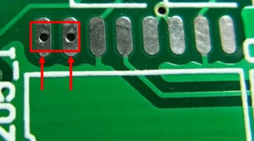
Can via holes be drilled in solder pads? If so, how can I fight it? When many people come into contact with the PCB, because the board space is too small and the devices are densely packed, the space is narrow and they cannot lead the holes. They will choose to drill the via holes on the pads, which makes the wiring much easier. But I am worried about whether it can be done in this way.

Can via holes be drilled on solder pads?
The answer is not recommended.
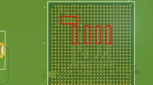
In the early days of PCB design, it was not allowed to have via holes on the BGA pads. The main reason was that the tin leakage would lead to insufficient solder paste on the pads, which would lead to virtual soldering and desoldering of the devices during device welding. Therefore, the devices were The holes are led out first and then drilled.

With the development of BGA, the spacing of BGA continues to shrink. By plugging resin holes, tin leakage will no longer occur. However, if the via hole is drilled on the pad, there is a risk of virtual soldering or falling off. The cost will increase and the impact will also be affected. The PCB board is beautiful, so this is not recommended.

The phenomenon of components standing up often occurs during the reflow soldering process of CHIP components (such as chip capacitors and chip resistors). The smaller the component size, the easier it is to occur, such as 0201, 0402 and other small chip components. During the reflow soldering process of the surface mount process, chip components produce a phenomenon as shown in the figure. A section of the component is lifted up, resulting in desoldering. Because of this situation, it is generally called the "tombstone" phenomenon.

The phenomenon of components standing up occurs because when the solder paste on the pads at both ends of the component is reflowed and melted, the surface tension of the two soldering ends of the component is unbalanced, and the end with greater tension pulls the component to rotate along its bottom.
This is also the reason why it is best not to drill via holes on the pads for some small package chip resistors and capacitors. The via holes are drilled on the edge of the pad. Due to the inconsistent tension at both ends of the pad, it is easy to cause tombstones.

Under what circumstances can via holes be drilled on the pads?
1.Buried blind holes
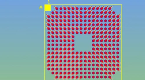
When the BGA pitch is less than or equal to 0.5mm, it is difficult to drill holes in the BGA. In this case, blind and buried vias can be used to solve the problem.
Blind vias: Blind vias are the type of vias that connect the inner PCB traces to the PCB surface traces. This hole does not penetrate the entire board. For example, only apply from the surface layer to the middle third layer.
Buried vias: Buried vias are the type of vias that only connect the traces between inner layers, so they are not visible from the PCB surface.
Since the blind holes only open from the surface layer to the inner layer, and not all of the PCB, there will be no leakage of tin, while the buried holes are drilled directly from the inside, so there is no such worry. The only problem is the cost. Considering this, the manufacturing cost of buried blind holes will increase greatly.
2.Thermal vias
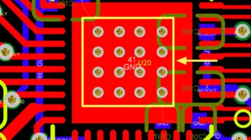
In PCB design, we often see the design as shown in the figure below. It is often seen in the recommended design of the chip. It is required to drill holes on the thermal pads. In this case, the thermal vias are drilled to dissipate heat from the IC.
Since there are no pins that need to be soldered in the middle of the chip body, there is no need to consider issues such as tin leakage and virtual soldering in the via holes on the IC heat dissipation pad.

Summarize
It is not recommended to drill PCB vias on the pads, as this will increase the chance of errors, affect the appearance, and cause components to stand up.
