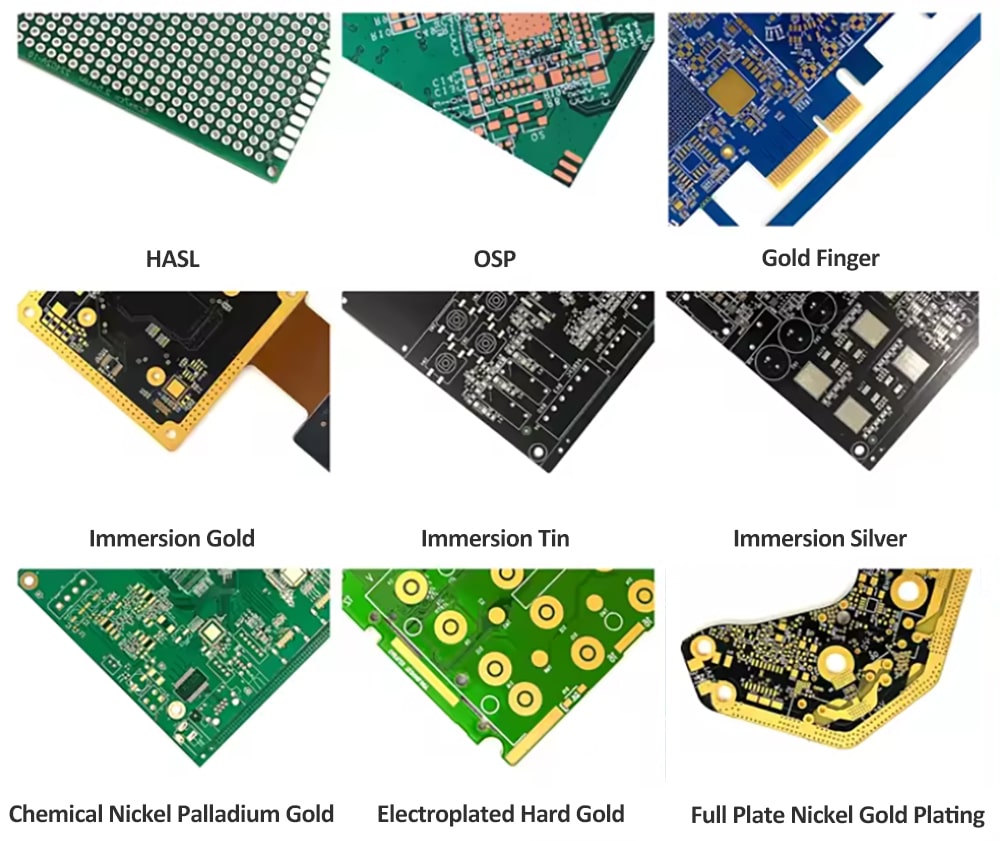
9 common PCB Surface Finishes processes
21 January 2025
Views: 1572
What are PCB Surface Finishes Processes?
The conductor of PCB is copper, but copper is very easy to oxidize in the air, which will affect the solderability of PCB. In order to ensure that the PCB has good welding and electrical properties, a Surface Finishes process is adopted for the conductor copper of the PCB. There are 9 common Surface Finishes processes, namely HASL, OSP, gold finger, immersion gold, immersion tin, and immersion silver, chemical nickel palladium gold, electroplated hard gold, full plate nickel gold planting.
Cost: Nickel gold plating>Immersed gold>Immersed silver>Immersed tin>Spray tin>OSP
Solderability: Nickel gold plating>HASL>OSP>ENIG>Immersed silver>Immersed tin
 HASL
HASL
HASL (Hot Air Solder Leveling) is a process that uses heated compressed air to level the PCB surface after coating it with molten tin-lead solder, so that a layer of coating layer can be formed on the PCB surface that can resist copper oxidation and provide good solderability. The thickness is approximately There are 7~11μm.
HASL is divided into lead spray tin and lead-free spray tin. The difference is that lead-free spray tin is more environmentally friendly and has a melting point of about 218 degrees; lead spray tin contains the harmful substance "lead" and has a melting point of about 183 degrees. The biggest advantage of HASL is that it is cheap and is a process chosen by many people.
OSP
The OSP (organic coating) process acts as a barrier layer between copper and air. It uses a chemical method to grow a layer of organic film with a thickness of 0.2-0.5μm on the bare copper surface of the PCB to protect the copper. Avoid oxidation. OSP's process is simple and low-cost, and it is also one of the most widely used processes.
Gold Finger
Goldfinger is not a processing method, but a general term for square pads arranged in rows and rows, which are commonly used in network cards, graphics cards and other products. The surface treatment method used for gold fingers is electroplating hard gold.
Immersion Gold
Immersion gold is also called soft gold, chemical gold, chemical nickel gold, chemical nickel gold, immersion nickel gold or electroless nickel gold. Plating this kind of gold on the bare copper of PCB can effectively prevent oxidation and protect the PCB for a long time. The method is to cover the surface of copper with a layer of this gold through a chemical reaction. The advantage is that nickel and gold can be attached to copper without complicated electroplating. The thickness is usually between 0.05~0.1um. Because precious metals are used, it is also a high-cost method.
Immersion Tin
Immersion tin is cheaper than immersion silver, has a smooth surface, is lead-free and is more environmentally friendly and is chosen by customers. However, when using the immersion tin process, the particles must be small enough and non-porous, and the tin thickness must be no less than 1.0μm to achieve better results.
Immersion Silver
Immersion silver provides a thin protective film for PCB through chemical replacement reaction, which can maintain good solderability in high temperature and humid environments. The copper surface is sealed by silver, which extends the service life and enhances solderability. The thickness is 0.1~0.4μm.
Chemical Nickel Palladium Gold
Compared with immersion gold, ENEPIG has an extra layer of palladium between nickel and gold. During the deposition reaction of gold replacement, the electroless palladium plating layer will protect the nickel layer and prevent it from being overly corroded by the replacement gold. ; The deposition thickness of nickel is generally 3~6μm, the thickness of palladium is 0.1~0.5μm, and the thickness of gold is generally 0.02~0.1μm. The cost of nickel-palladium gold is higher than that of immersion gold.
Electroplated Hard Gold
Electroplated hard gold consists of a layer of gold plated on a nickel coating. The purity of hard gold is 99.6% and has high hardness. It is used in areas with frequent plugging and unplugging wear, such as edge connector fingers, such as gold fingers.
Full Plate Nickel Gold Planting
As the name suggests, nickel-gold plating is used on a large area and the cost is high.
Share This Story, Choose Your Platform!
