Web Analytics Made Easy - Statcounter
PCB Manufacturing | POE PCB
This website uses cookies:
Our website use cookies to analyze website accesses and improve your online experience. By continuing browsing this website,you agree to our use of cookies and privacy policy.
Accept all cookies
Decline
This website uses cookies:
Our website use cookies to analyze website accesses and improve your online experience. By continuing browsing this website,you agree to our use of cookies and privacy policy.
Accept all cookies
Decline
Get A Quote
Get A Quote
Worried About Surprise Tariffs? We Cover It, $0 to You.
×

PCB MANUFACTURING
SERVICES

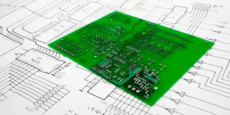
Advanced PCB fabrication from prototype to mass production

20+Years PCB Experience
50M+PCBs Manufactured
99.8%First Pass Yield

PCB MANUFACTURING EXCELLENCE

Layer Count

1-40 Layers

Single to 40-layer PCB manufacturing capability

Board Thickness

0.2-6.0mm

Flexible thickness range for various applications

Min Trace Width

0.075mm

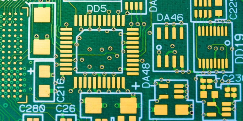
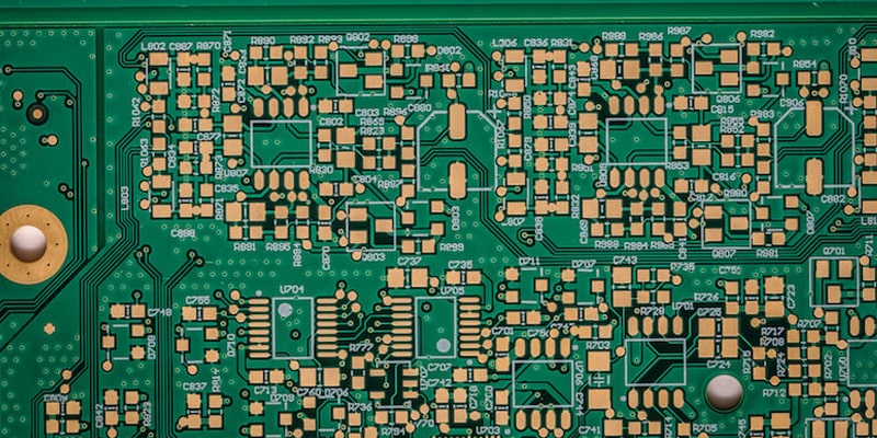
Ultra-fine trace capability for HDI designs

Min Via Size

0.1mm

Micro via technology for high-density interconnect

Copper Weight

0.5-10oz

Standard to heavy copper for power applications

Surface Finish

HASL/ENIG/OSP

Multiple surface finish options available

Tolerance

±0.05mm

High precision manufacturing tolerance

Max Board Size

610×1200mm

Large format PCB manufacturing capability

Lead Time

24H-7 Days

Fast prototype to production turnaround

PCB MANUFACTURING FACILITY

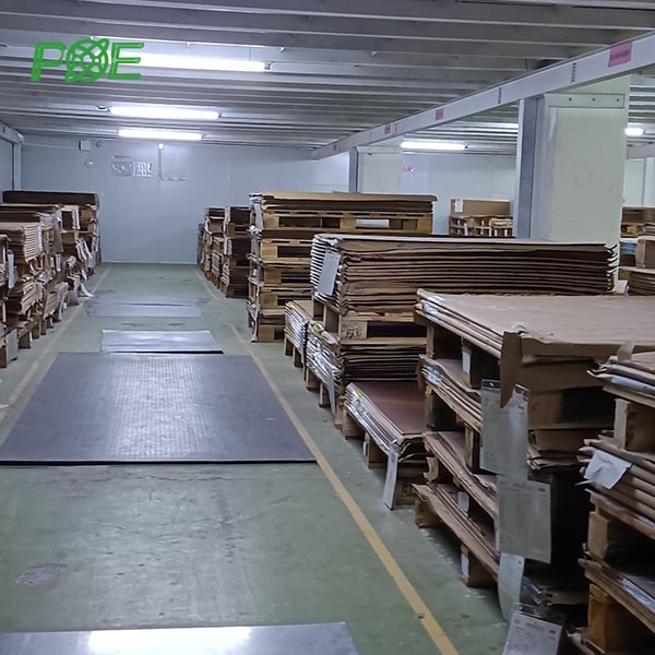
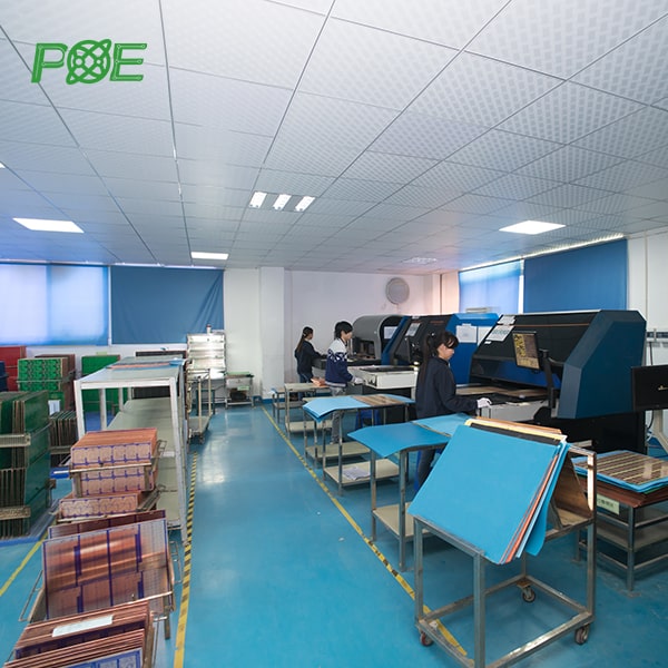
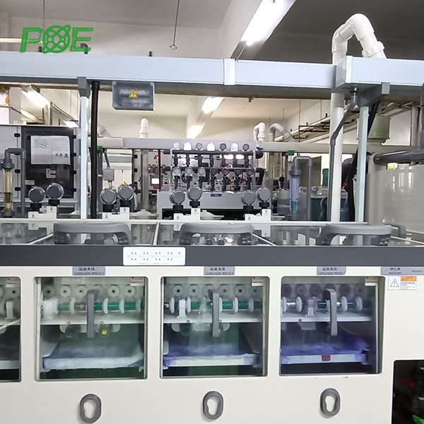
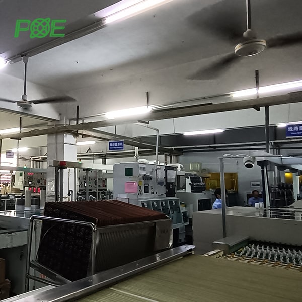
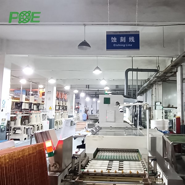
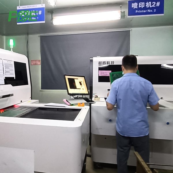
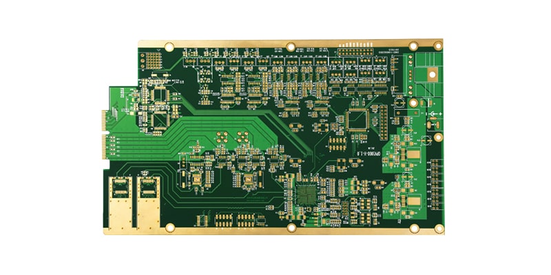
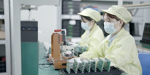
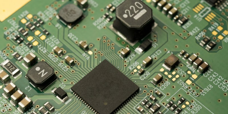
Our state-of-the-art PCB manufacturing facility spans 15,000 square meters with advanced production lines capable of producing single-layer to 40-layer PCBs. Equipped with the latest HDI technology, multilayer lamination systems, and precision drilling equipment, we serve industries requiring the highest quality standards. Our PCB manufacturing capabilities include rigid PCBs, flexible PCBs, rigid-flex combinations, and specialty materials like Rogers, Polyimide, and ceramic substrates for high-frequency and high-temperature applications.

PCB MANUFACTURING PROCESS

PCB Substrate Cutting

Material

Premium FR4 substrate preparation and cutting

Inner Layer Processing

Inner layer Exposure

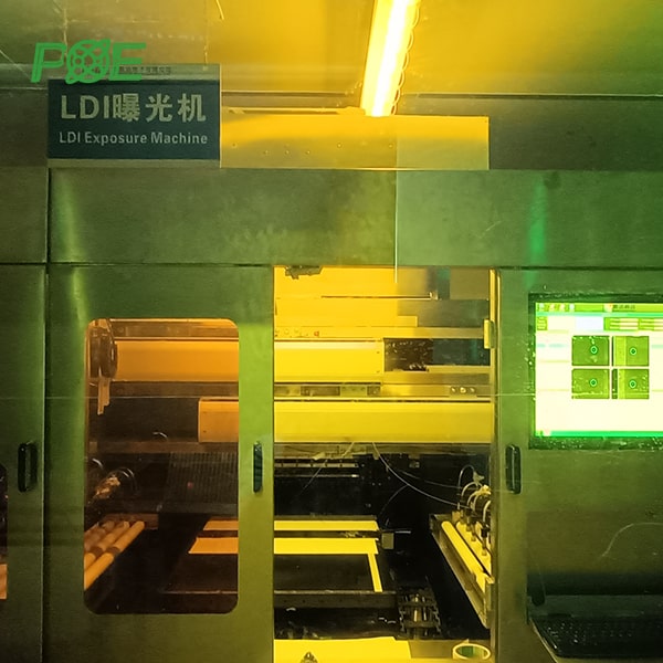
UV lithography for inner layer patterning

Photolithography

Inner Layers Dry film imaging

Photoresist application and exposure process

Chemical Etching

Inner Layers Etching

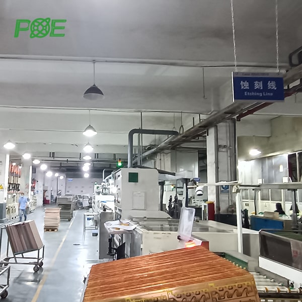
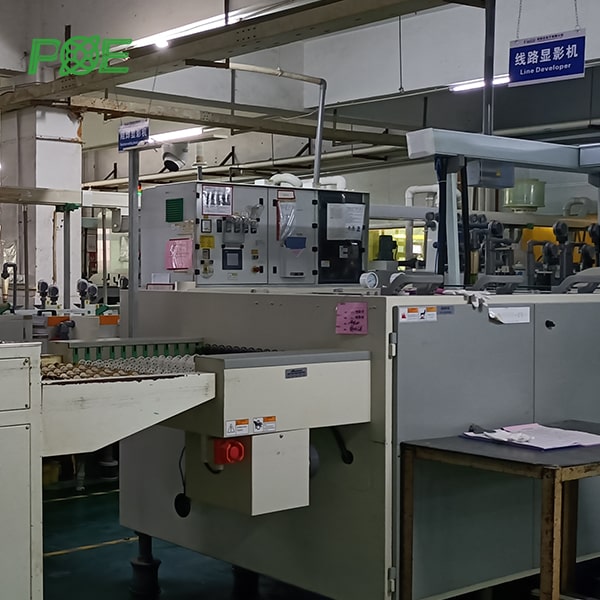
Chemical removal of unwanted copper traces

Inner Layers Inspection (AOI)

Automated optical verification of inner circuits

Multilayer Lamination

Chemical Etching Line

Oxide treatment for layer adhesion

CNC Drilling

Lamination Layerstack

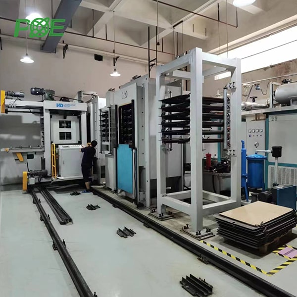
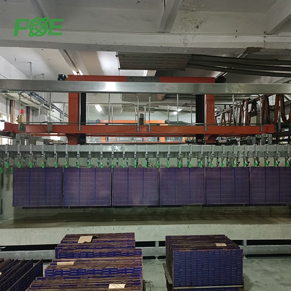
Multi-layer PCB pressing and bonding

Plated Through Holes

Drilling

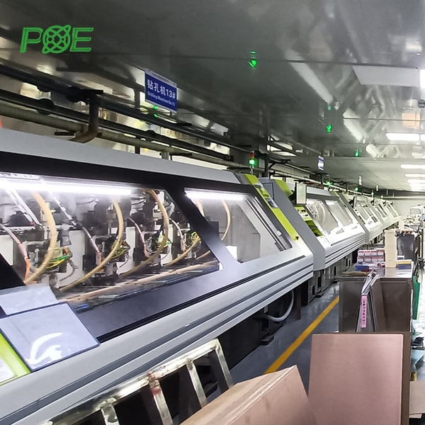
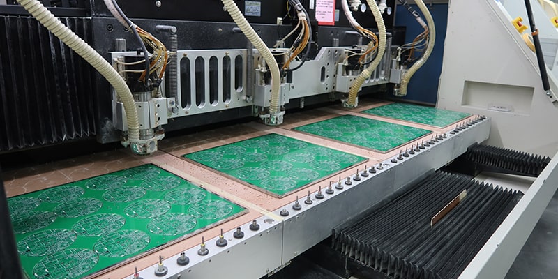
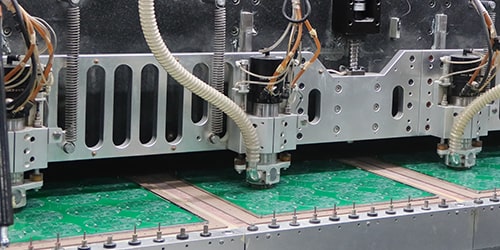
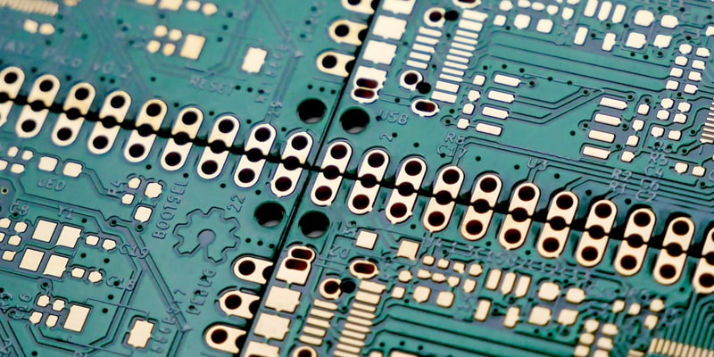
High-precision via and mounting hole drilling

Outer Layer Processing

Film Drop

Photoresist removal after processing

Solder Mask Application

PTH

Plated through-hole copper deposition

Silkscreen Printing

Outer Layers Dry film imaging

External layer photoresist patterning

Surface Finish

Copper Plating (PTH)

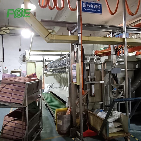
Electroplating copper in drilled holes

CNC Routing

Outer Layers Etching

Final copper trace definition and cleaning

Electrical Testing

Outer Layers Inspection (AOI)

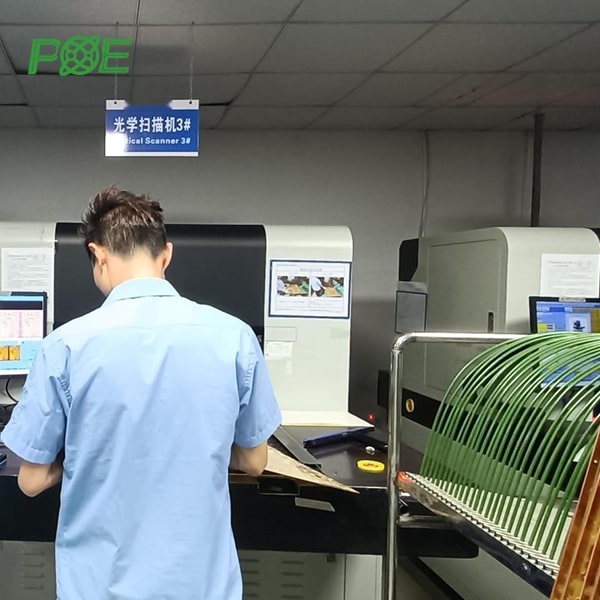
Final circuit pattern verification

X-ray Inspection

Inner circuit Xray

X-ray inspection of internal connections

Impedance Testing

Solder Mask

Protective coating application and curing

Final Inspection

Silkscreen

Component legends and marking printing

Packaging

Vacuum Packaging

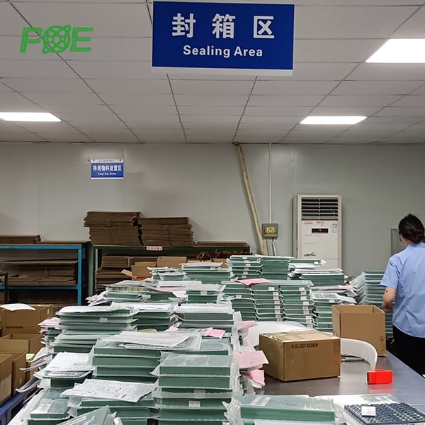
Moisture-free protective packaging

PCB MANUFACTURING CAPABILITIES

Standard PCB

Standard PCB

1-40 layer standard PCB fabrication with fast turnaround

Learn More
HDI PCB

HDI PCB

High Density Interconnect with microvias and fine pitch

Learn More
Rigid-Flex PCB

Rigid-Flex PCB

Complex rigid-flex designs for space-constrained applications

Learn More
Multilayer PCB

Multilayer PCB

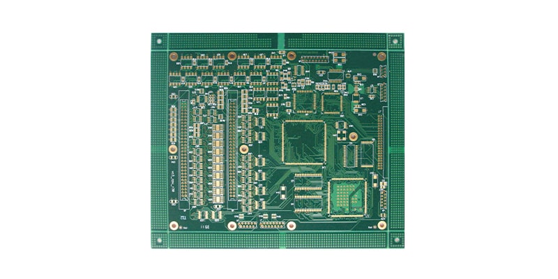
Up to 40-layer complex PCB manufacturing

Thick Copper PCB

Thick Copper PCB

Heavy copper PCB for high-current applications

High Frequency PCB

High Frequency PCB

Rogers and PTFE materials for RF applications

Flexible PCB

Flexible PCB

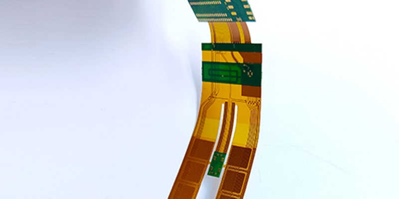
Single and multilayer flexible circuit boards

Metal Core PCB

Metal Core PCB

Aluminum and copper core for thermal management

Ceramic PCB

Ceramic PCB

High-temperature ceramic substrate solutions

Via-in-Pad PCB

Via-in-Pad PCB

Advanced via-in-pad technology for BGA designs

Blind Buried Via

Blind/Buried Via

Complex via structures for high-density designs

Impedance Control

Impedance Control

Precise impedance matching for high-speed signals

PCB Prototyping

PCB Prototyping

Rapid prototyping from 24 hours

PCB Assembly Ready

Assembly Ready PCB

PCBs optimized for automated assembly

ADVANCED TECHNOLOGY

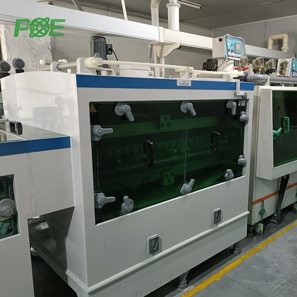
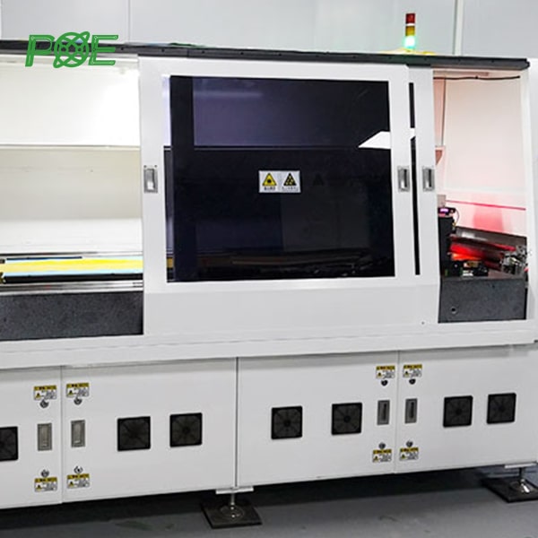
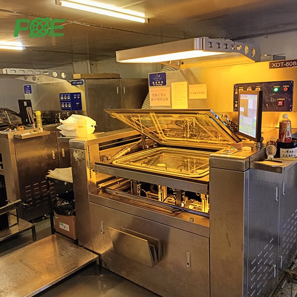
State-of-the-art PCB manufacturing equipment and processes

FAST DELIVERY

24H prototype, 3-5 days production, express options available

QUALITY CERTIFIED

IPC Class 2/3, ISO9001, UL certified manufacturing

DESIGN SUPPORT

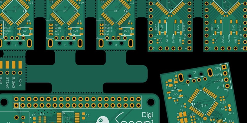
DFM analysis and PCB layout optimization services

PCB MANUFACTURING CERTIFICATIONS

ISO 9001:2015
ISO 14001:2015
ISO 13485:2016
RoHS
Reach
UL
IPC-A-610
IPC-A-600


PCB CLIENT TESTIMONIALS

"

Outstanding PCB quality and precision. Their HDI technology perfectly met our miniaturization requirements.

Jennifer Wang Electronics Design Engineer
"

Excellent rigid-flex PCB manufacturing. Fast turnaround and superior quality for our wearable devices.

Robert Kim Product Development Manager
"

Reliable PCB partner for our automotive electronics. Consistent quality and on-time delivery.

Maria Garcia Automotive Systems Director