What is the purpose of each layer of the circuit board?
21 January 2025
Views: 2822
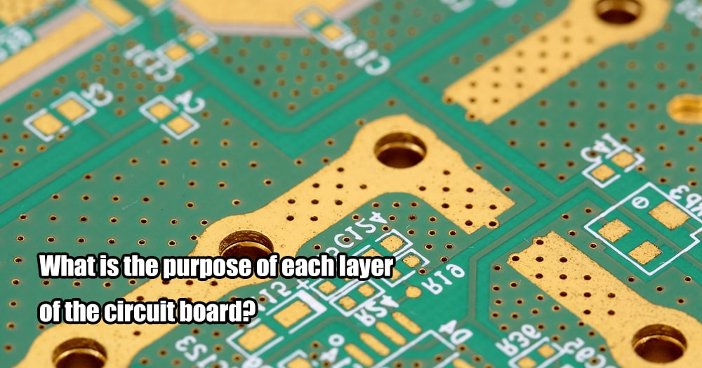
A printed circuit board (PCB) is composed of multiple layers, and the layer classification mainly refers to the number of electrical layers. Non-electrical layers are also present in almost every PCB. So, what is the function of each layer in a PCB?
1.Mechanical Layer:
As the name suggests, the mechanical layer is used for mechanical shaping, which refers to the outer appearance and structure of the entire PCB board. When we talk about the mechanical layer, we are referring to the overall shape and structure of the PCB. The term "mechanical" emphasizes that it does not have electrical properties, so it can be safely used for drawing outlines, mechanical dimensions, placing text, and other tasks without worrying about affecting the electrical characteristics of the board. It can also be used for designing physical mechanical properties such as borders, slots, holes, data labeling, assembly instructions, and more.
There can be multiple mechanical layers, and their functions can be customized, including dimension labeling and other purposes. These specifications may vary depending on the requirements of the design company or PCB manufacturer. Additionally, mechanical layers can be superimposed on other layers for combined output and display.
2.Silkscreen Layer:
The silkscreen layer is divided into the top overlay (top silkscreen) and bottom overlay (bottom silkscreen), used to define the silkscreen characters on the top and bottom layers. The silkscreen layer is primarily used for placing printed information, such as component names, component symbols, component pins, component outlines and labels, various annotation characters, copyrights, etc. This information facilitates circuit soldering and troubleshooting in the future.
3.Keep-Out Layer:
The keep-out layer is used to define the areas on the PCB where components and traces can be effectively placed. A closed region is drawn on this layer as the valid routing area. The keep-out layer is mainly used for constraining specific areas, such as areas where copper should not be placed or where no traces or vias are allowed. Automatic layout and routing cannot be performed outside this area.
Sometimes, people mistakenly use the keep-out layer as a mechanical layer. However, this is incorrect, and it is recommended to differentiate between them to avoid attribute changes during production.
4.Signal Layer:
The signal layer is primarily used for routing wires on the PCB. It includes the top layer and bottom layer, which are electrical layers where components can be placed and traces can be routed. The top layer and bottom layer accommodate components, while inner layers are used for routing.
5.Solder Paste Layer:
The solder paste layer is divided into the top paste and bottom paste layers. It is also known as the stencil layer or solder paste layer. The solder paste layer is used during machine assembly and corresponds to the solder pads of all surface-mounted components. It is the same size as the top and bottom layers and is used for creating a stencil for solder paste application. Generally, a layer of solder or gold on the solder pads of a PCB is the solder paste layer. It assists in the soldering process, making it easier to solder the components. In the design, the solder paste layer is positive, meaning that solder paste is applied where the drawings are present and not applied where there are no drawings.
6.Solder Mask Layer:
The solder mask layer is divided into the top solder mask and bottom solder mask layers. The green oil (or other colors, commonly green, blue, black, white, red, yellow) on the surface of a PCB is the solder mask layer, which provides insulation. In reality, the solder mask layer utilizes negative output. So, when the shape of the solder mask layer is mapped onto the board, it exposes the copper instead of covering it with solder mask. The term "opening the solder mask layer" refers to creating openings on the solder mask layer. Regular copper traces or wiring are typically covered by solder mask. If the solder mask layer is modified accordingly, it prevents the solder mask from covering those areas, exposing the copper.
7.Internal Power/Ground Layer:
This type of layer is used only in multilayer boards and is primarily used for routing power and ground lines. The term "double-layer board," "four-layer board," "six-layer board" generally refers to the number of signal layers and internal power/ground layers.
8.Assembly Layer:
The assembly layer is divided into the top assembly and bottom assembly layers. It is typically used during PCBA (Printed Circuit Board Assembly) processes. The assembly layer is used to indicate the position and orientation of component assembly, representing the physical size of the components. It is mainly used during surface mount assembly.
9.Drill Layer:
The drill layer includes the drill grid and drill drawing layers, which provide information about drill holes during the PCB manufacturing process (e.g., for solder pads and vias).
10.Multilayer:
For components and through-hole vias that need to penetrate the entire PCB, establishing electrical connections with different conductive layer patterns, there is a dedicated abstract layer called the multilayer. Generally, solder pads and vias are placed on the multilayer. If this layer isused, it will be specified in the PCB design and manufacturing process to ensure proper connectivity.
These are the main layers typically found in a printed circuit board (PCB). The specific layers used in a PCB design can vary depending on the requirements of the circuit and the design constraints. It's important to consider the functionality and electrical properties of each layer when designing a PCB to ensure proper circuit operation and manufacturability.
