Common surface treatment processes for PCB
12 December 2025
Views: 761
Why Perform Special Treatments on PCB Surfaces?
Copper oxidizes easily in air, and the oxide layer significantly impacts soldering, leading to issues like cold joints or false soldering. In severe cases, it may prevent proper bonding between pads and-components. To address this, a protective coating is applied (or plated) onto the pad surfaces during PCB manufacturing to prevent oxidation.

Key Factors to Consider When Selecting PCB Surface Treatment Processes
The choice of surface treatment is a critical step in PCB production, affecting soldering performance, conductivity, corrosion resistance and cost. Below are key factors to consider:

Product Requirements and Operating Environment
Product Needs: Different electronics have varying performance demands. Consumer electronics prioritize cost and mass production, while high-end products like aerospace equipment focus on reliability. Select a surface treatment based on specific product requirements.
Operating Environment: Environments with high humidity, temperature, or corrosive elements require robust treatments like ENIG (Electroless Nickel Immersion Gold) or OSP (Organic Solderability Preservative).
Soldering Performance and Reliability

Soldering Performance: Different treatments affect soldering differently. For example, HASL (Hot Air Solder Leveling) offers excellent solderability but uneven surfaces, making it unsuitable for high-density PCBs.
Reliability: High-reliability applications (e.g., automotive or medical devices) often use ENIG due to its oxidation resistance and long shelf life.
Cost Control
Cost: HASL and OSP are low-cost options for mass production, while ENIG, immersion silver, and immersion tin are pricier but offer superior performance.
Production Volume: For prototypes or small batches, low-cost processes like HASL are ideal. For large volumes, high-end treatments may provide better long-term value despite higher initial costs.
Appearance and Testing Requirements
Appearance: ENIG provides a smooth, shiny finish for high-end products.
Testability: Silver immersion ensures excellent conductivity for signal-sensitive boards.
Environmental and Process Complexity
Environmental Regulations: Lead-free HASL complies with RoHS standards.
Process Complexity: ENIG and immersion tin involve complex steps, impacting production efficiency.
Common PCB Surface Treatment Processes

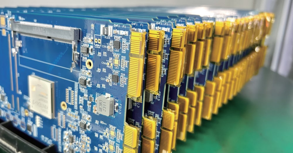
1.Gold Finger (Hard Gold Plating)
Process: Electroplated nickel-cobalt alloy (2-30μm thick).

| Features |
|
Wear resistance: Survives 100+ insertion cycles.
Oxidation resistance: Maintains conductivity in air.
High cost: Thick gold layer increases material expenses.
Applications: PCle slots, memory modules, high-frequency connectors.
|
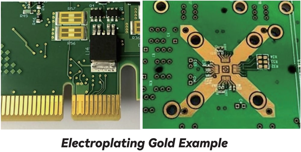
2.Electroplating Gold
Process: Electroplated hard gold (1-5μm, cobalt/nickel alloy) or soft gold (0.05-0.2μm, pure gold).

| Features |
|
High conductivity: Ideal for 5G/RF circuits.
Solder compatibility: Soft gold bonds well but risks "gold embrittlement."
High cost: Depends on gold thickness and area.
Applications: Aerospace, medical devices, chip-on-board (COB).
|
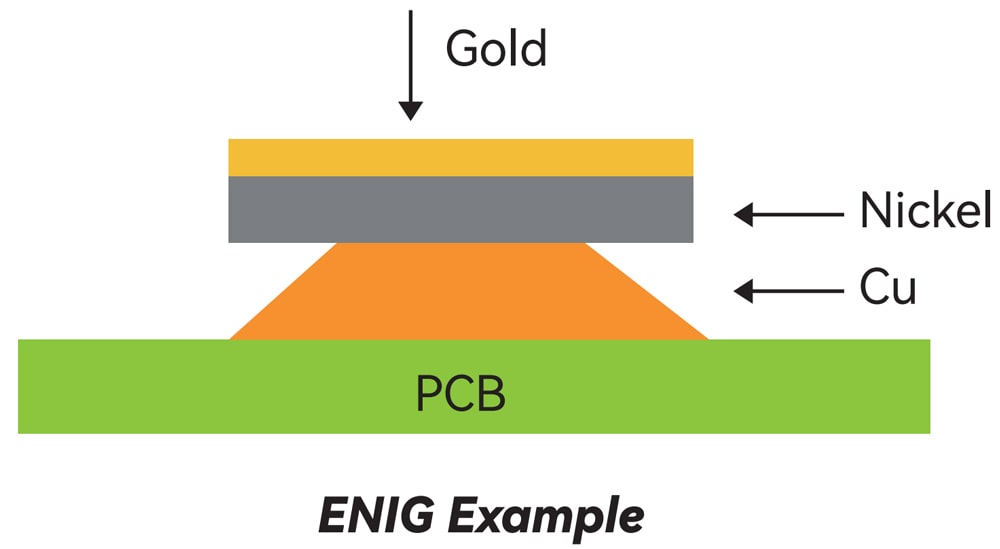
3. ENIG (Electroless Nickel Immersion Gold)
Process: Chemical nickel (3-5μm)+immersion gold (0.05-0.1μm).

| Features |
|
Flat surface: Suitable for BGA and 0201 components.
Oxidation resistance: Nickel barrier +gold protection.
Moderate cost: Thinner gold layer reduces expenses.
Black pad risk: Poor nickel-phosphorus control may cause soldering failures.
Applications: Consumer electronics, SMT processes requiring multiple reflows.
|
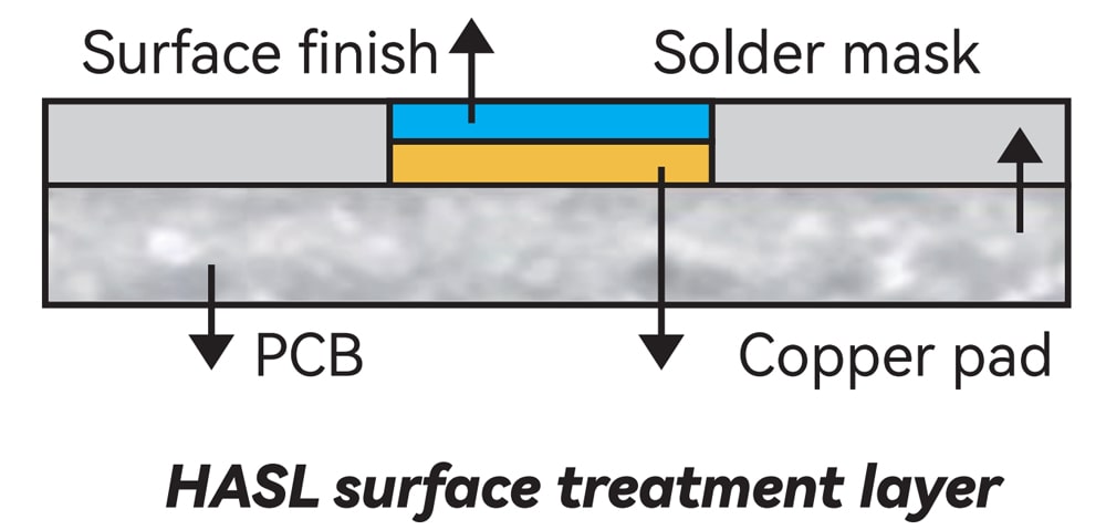
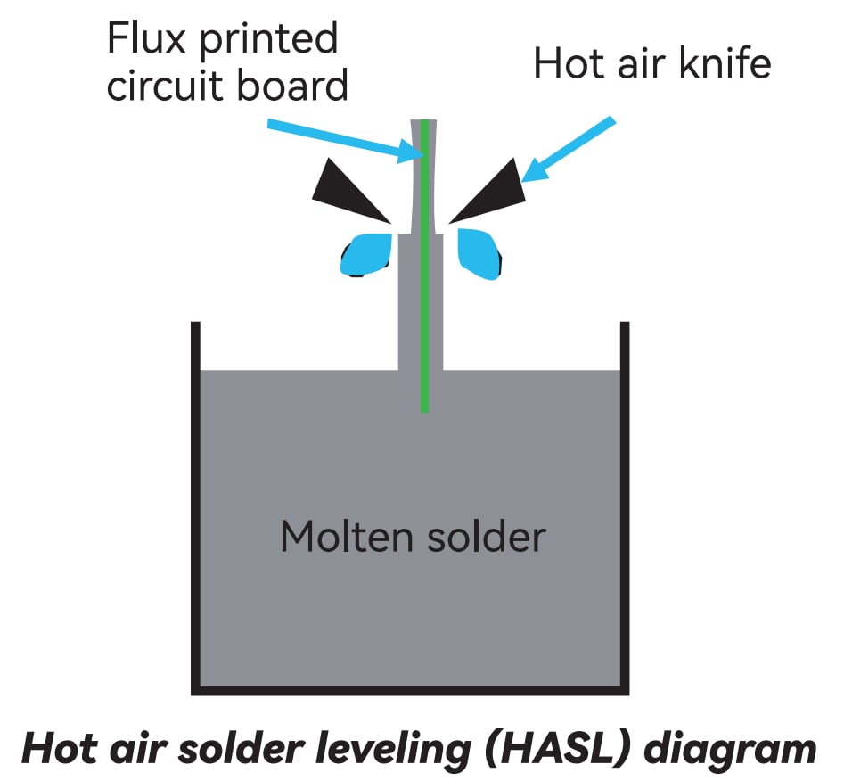
4.HASL (Hot Air Solder Leveling)
Process: Molten tin-lead or lead-free alloy sprayed onto copper, leveled with hot air.
| Types |
|
Leaded HASL: Sn/Pb alloy (e.g., Sn63Pb37), low cost.
Lead-free HASL: SAC alloy (RoHS-compliant).
|

| Features |
|
Lowest cost: Ideal for high-volume production.
Uneven surface: Not suitable for fine-pitch components (<0.4mm QFP).
Short shelf life: 6-12 months due to oxidation.
Applications: Low-density PCBs, lighting, cost-sensitive devices.
|
Key Comparison Table:
| Features |
Gold finger (hard gold) |
Gold plating (soft gold) |
Immersion gold (ENIG) |
HASL |
| Thickness |
2-30μm |
0.05-0.2μm |
0.05-0.1μm |
10-40μm |
| Hardness |
High (containing cobalt/nickel) |
Low (pure gold) |
Medium (nickel bottom layer) |
Low (pure tin) |
| Surface flatness |
General |
High |
Very high |
Low (orange peel effect) |
| Weldability |
Welding is not recommended |
Excellent (need to prevent gold embrittlement) |
Excellent |
Excellent (but need to prevent oxidation) |
| Cost |
Highest |
High |
Medium |
Lowest |
| Applicable scenarios |
High-frequency plug-in interface |
High-frequency signal, chip binding |
High-density pads, BGA |
Low cost, large pads |
Selection Recommendations
Gold Finger: Frequent insertion (e.g., server RAM) or high-frequency signal transmission.
Electroplated Gold: High-reliability scenarios (aerospace, medical) or wire bonding.
ENIG: High-density designs (smartphone motherboards), multi-reflow SMT processes.
HASL: Cost-sensitive projects (power boards, LED lighting).
 Choosing the right surface treatment ensures performance, reliability, and cost-effectiveness. By fully considering product requirements, operating environment, welding performance, cost control, appearance requirements and environmental protection, POE can provide the best surface treatment process for different applications to ensure smooth production.Choosing the right surface treatment ensures performance, reliability, and cost-effectiveness. By fully considering product requirements, operating environment, welding performance, cost control, appearance requirements and environmental protection, POE can provide the best surface treatment process for different applications to ensure smooth production
