
From 3 oz to 20 oz copper weight. Engineered for power electronics, EV charging, industrial inverters, and aerospace systems where standard PCBs cannot carry the current load.
Standard copper traces cannot handle high continuous currents without thermal failure. These industries depend on heavy copper to deliver reliable, long-service electronics.
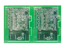
8L/ FR4 Tg150/ 4oz/ 1.6mm/ ENIG
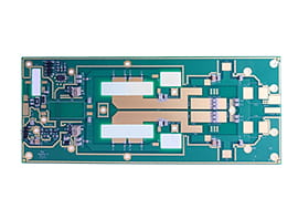
2L/ FR4/ 1.6mm/ 3oz/ ENIG/ 3u''Green Soldermask/ White silkscreen
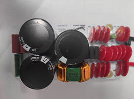
2L/ FR4-TG180/ 2.4mm/ 4oz/ ENIG/ White-Soldermask/ black-silkscreen
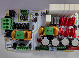
2L/ FR4-TG180/ 2.4mm/ 4oz/ ENIG/ White-Soldermask/ black-silkscreen
Standard PCB copper (1 oz = 35μm) has a hard limit on current-carrying capacity. Beyond that limit, trace heating causes delamination, solder joint fatigue, and insulation breakdown — all failure modes with catastrophic consequences in power electronics.
| Parameter | Standard (1–2 oz) | Heavy Copper (3–20 oz) |
|---|---|---|
| Copper Thickness | 35–70 μm | 105–700 μm |
| Current Capacity | Up to ~10A | Up to 200A+ |
| Thermal Dissipation | Limited | Excellent |
| Mechanical Strength | Standard | Significantly higher |
| Via Current Rating | Low | High (filled/plated) |
| PCB Lifespan | Standard | Extended under load |
Thick copper layers act as heat spreaders, distributing thermal loads across the board and reducing hotspot temperatures by up to 40% compared to equivalent trace widths in standard copper.
Heavy copper allows high-current traces to be routed at narrower widths, enabling more compact designs without compromising current capacity or thermal performance.
Reduced thermal cycling stress and lower operating temperatures mean heavy copper PCBs maintain electrical integrity over longer service lives — critical for infrastructure and safety-critical applications.
We support mixed-copper-weight boards: heavy copper on power layers for current carrying, standard copper on signal layers for fine-pitch routing — all in one stackup.
All specifications below reflect verified production capability, not advertised limits.
| Parameter | Specification |
|---|---|
| Copper Weight | 3 oz to 20 oz (105 μm to 700 μm); mixed-weight stackups available |
| Layer Count | 1 to 20 layers; HDI with heavy copper available on request |
| Min Trace Width | 5 mil (3–6 oz); 8 mil (7–12 oz); 12 mil (13–20 oz) |
| Min Trace Space | 5 mil (3–6 oz); 8 mil (7–12 oz); 12 mil (13–20 oz) |
| Board Thickness | 0.8 mm to 6.5 mm |
| Max Board Size | 610 × 1200 mm |
| Base Material | FR4, High-Tg FR4, Rogers, Polyimide, Metal Core (MCPCB) |
| Surface Finish | HASL, ENIG, OSP, Immersion Ag/Sn, Hard Gold |
| Solder Mask | LPI both sides; window-opening available for bus bars |
| Hole Size (Min) | 0.3 mm mechanical; via fill and copper plugging available |
| Copper Fill / Plugging | Via copper filling, thermal via arrays, copper-filled blind vias |
| Current Standard | IPC-2152 current-carrying capacity calculation |
| Quality Standard | IPC-A-600 Class 2 / Class 3; ISO 9001:2015 |
| Prototype Lead Time | 5–7 days (standard); expedite available on request |
* Minimum feature sizes and tolerances vary by copper weight. DFM review included with every order.
Heavy copper fabrication requires different process controls than standard PCBs. The thick copper introduces unique challenges in etching, lamination, and dimensional control that we have solved through years of production experience.
Standard single-step etching cannot achieve accurate trace definition on copper over 3 oz. We use a step-etching process — building copper in multiple plating passes and etching in controlled stages — to maintain trace edge definition and spacing accuracy at high copper weights.
Thick copper layers create significant height differentials at trace edges. Our lamination process uses customised prepreg combinations and precisely controlled pressure and temperature profiles to eliminate voids and ensure consistent dielectric thickness across the panel.
Thermal vias and through-holes in heavy copper boards require copper filling or plugging to maximise current-carrying capacity and thermal conductivity. We offer electroplated copper via fill, resin fill + copper cap, and open via arrays for thermal dissipation.
Applying solder mask over thick copper features requires specialised LPI application techniques to achieve full coverage and adhesion at trace edges without bridging. We verify mask thickness and adhesion with cross-section analysis on every production run.
Every heavy copper order receives a Design for Manufacturability review covering trace width vs copper weight compatibility, via aspect ratios, solder mask clearance, and thermal relief pad design. Issues are resolved before production, not during.
100% electrical test (flying probe or fixture) on every panel. AOI for outer layer verification. Cross-section analysis available on request for copper thickness verification and void inspection. Full inspection reports provided with every shipment.
 Email: all@poe-pcba.com
 Whatsapp: 85292069596
 Tel: 0755-25312250/ +8613798543496
 Factory Address: Floor 3, Jinyuan Industrial Park, No. 56, Tangtou Avenue, Shiyan Town, Baoan District, Shenzhen China





