People mix up three terms — bare, blank, unpopulated — they mean the same thing in procurement. "PCBA" or "populated board" is the next stage: same board, components mounted.
Substrate and layer stack
The base is laminate (FR-4 is the default; polyimide, Rogers, or aluminum for special jobs). Layer count runs from 1 to 40+; your Gerber and stack-up file decide that, not the fabricator.
For buying: layer count and thickness (0.8 / 1.0 / 1.6 mm typical) drive price more than anything except size. A 4-layer 100×100 mm FR-4 board and a 10-layer same-size board are different animals on the same drawing.
Copper and traces
Copper weight is usually 1 oz/ft² (35 µm) outer, sometimes 0.5 oz inner or 2 oz for power. Trace width and spacing (commonly 6/6 mil, down to 3/3 mil for HDI) are design-bound but matter to yield: tighter rules = more likely a batch fails electrical test.
Procurement tip: if your designer hands you 4/4 mil rules on a cost-sensitive board, expect the bare-board quote to jump 20–40% versus 6/6.
Surface finish
This is the coating on exposed copper pads. Bare copper oxidizes in weeks; finish keeps it solderable. Three you will see on quotes:
HASL / Lead-free HASL — cheapest, slightly uneven surface, fine for through-hole and coarse pitch. Shelf life ~12 months.
ENIG — flat gold over nickel, mandatory for BGA/fine-pitch under 0.5 mm, ~12 month shelf life, +30–60% cost vs HASL. Watch "black pad" risk, pick a shop that controls the bath.
OSP — thin organic film, flat, cheap, but 6–12 month shelf life and dies after 1–2 reflows. Good only if you assemble fast.
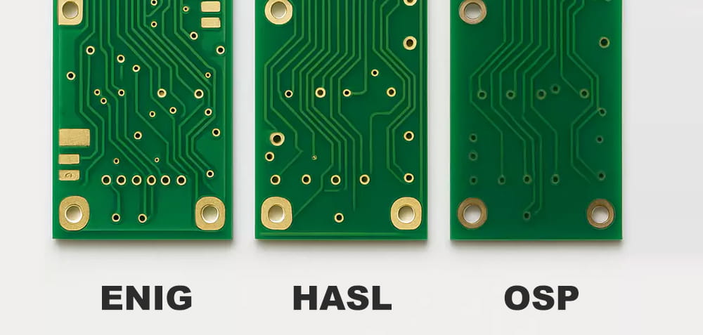
Do not let the factory "pick whatever." Finish choice locks your assembly window and storage life.
Solder mask and silkscreen
Solder mask is the green (or black/blue/red) coating that stops solder bridging. Silkscreen is the white text. On a bare board these are cosmetic-to-functional: a missing mask between fine-pitch pads is a reject, not a blemish.
Buyers rarely specify color, but if your assembly house uses AOI or manual inspection, green still gives the best contrast. Matte black looks sharp, photographs badly on the line.
Holes and vias
Drilled holes come plated (PTH) or unplated (NPTH for screws/fixtures). Blind/buried vias live inside multilayer stacks and push cost and lead time up sharply.
For an unpopulated board, the drill drawing and Excellon file are part of the spec. If your quote says "blind via" but your design has none, someone misread the stack-up.
Electrical test and acceptance
A bare board is tested for continuity and isolation — flying probe or fixture — not for function. You will not know if your circuit "works," only that traces connect where they should and don't where they shouldn't.
Ask for the test report (netlist pass/fail, coupon cross-section if impedance-controlled). If a supplier ships without an e-test stamp on the traveling card, treat it as uninspected.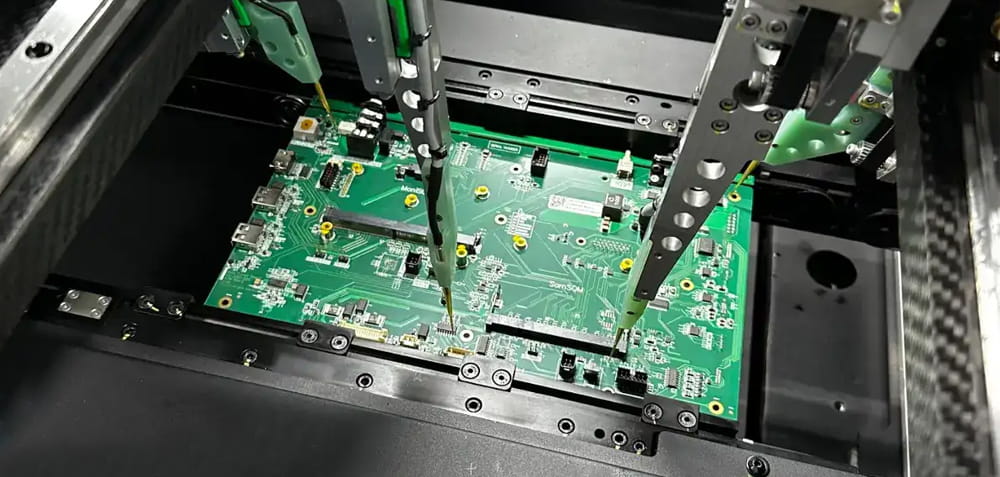
Panelization
Bare boards almost never ship as single pieces at volume; they come in panels with breakaway tabs, V-cut, or routed edges. Your pick-and-place house cares about panel size (usually 200×300 mm or 250×350 mm), fiducials, and tab strength.
Specify panel drawing or accept the fab's default — but know that a wrong panel edge can jam an SMT line later. This is decided at bare-board stage, not assembly stage.
Storage and handling before assembly
Unpopulated does not mean indestructible. FR-4 drinks moisture; ENIG tarnishes slowly; OSP rots in humidity; static hurts nobody on a bare board except it ruins OSP or silver finish if handled carelessly.
Store in moisture-barrier bags with desiccant at 15–25 °C, 30–60 % RH. Keep ESD shielding bags for boards with immersion silver or tight-pitch ENIG pads. Rotate stock — OSP boards older than 6 months go to scrap quietly.
Why this matters to a buyer?
When you request "PCB quote," you are buying an unpopulated board defined by: size, layers, material, copper weight, finish, mask color, hole count, tolerance class (IPC-6012 Class 2 is the normal commercial bar), and test method. Miss one, and two shops return prices 2× apart for "the same board."
If you only ever compare the bottom-line number, you will drift toward the shop that dropped ENIG to HASL, widened the drill tolerance, or skipped e-test. The cheap bare board becomes an expensive populated scrap lot.
We fabricate unpopulated PCBs from 1–20 layers, FR-4 / Rogers / polyimide, with HASL, LF-HASL, ENIG, OSP, and immersion silver, IPC-6012 Class 2/3, e-tested, panelized to your SMT house's frame. If you want a second quote on your current bare-board spec — or a sanity check on whether your finish choice matches your assembly plan — send the Gerber and stack-up, we will tell you where the spec is costing you money before you place the order.

 Email: all@poe-pcba.com
 Whatsapp: 85292069596
 Tel: 0755-25312250/ +8613798543496
 Factory Address: Floor 3, Jinyuan Industrial Park, No. 56, Tangtou Avenue, Shiyan Town, Baoan District, Shenzhen China





