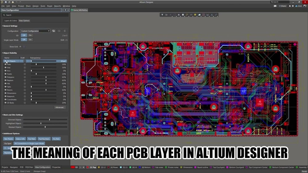
| Name | Definition |
| Top Layer | Mainly used for wiring and placing components. Note: Single panel does not have a Top layer |
| Bottom Layer | |
| Mid Layer | Used to lay signal lines in multi-layer boards, which can have up to forty layers. |
| Mechanical | Define the size of the PCB physical borders |
| Top silk screen layers | The top and bottom silk screen layers are mainly used to mark component numbers, characters, trademarks and other logos. |
| Bottom silk screen layers | |
| Top Paste | Also called stencil layer. The function is to stick the stencil to the original, which can be fully compatible with the solder mask layer |
| Bottom Paste | |
| Top Solder | The non-solderable layer in the PCB is used to protect the copper foil from being oxidized and covered with tin, etc. The solder resist is painted on the PCB. |
| Bottom Solder | |
| Drill Guide | Center positioning coordinate layer for drilling of pads and vias |
| Drill Drawing | Drilling size of pads and vias Aperture size description layer |
| Keep_Out Layer | An area on a circuit board where components and routing can be efficiently placed. Draw a closed area on this layer as the effective routing area. Automatic layout and routing cannot be performed outside this area. |
| Muliti_Layer | The pads and through-holes on the circuit board need to penetrate the entire circuit board and establish electrical connections with different conductive pattern layers. Therefore, the system specifically sets up an abstract layer and multiple layers. Generally, the pads and vias are arranged on multiple layers. If this layer is closed, the pads and vias cannot be displayed. |
SMT speed ≠ PCBA lead time. ⏱
— POE PCB/PCBA Manufacturer (@poe_pcba) May 13, 2026
The clock is usually set by materials/BOM, stencil prep, first-run tuning, inspection slots, rework handling, and final test.
At POE, we front-load checks and align these gates early—so builds flow from release → shipment without surprise delays. pic.twitter.com/H5ESaGgO0z
 Email: all@poe-pcba.com
 Whatsapp: 85292069596
 Tel: 0755-25312250/ +8613798543496
 Factory Address: Floor 3, Jinyuan Industrial Park, No. 56, Tangtou Avenue, Shiyan Town, Baoan District, Shenzhen China


