Our website use cookies to analyze website accesses and improve your online experience. By continuing browsing this website,you agree to our use of cookies and privacy policy.
Accept all cookies
Decline
This website uses cookies:
Our website use cookies to analyze website accesses and improve your online experience. By continuing browsing this website,you agree to our use of cookies and privacy policy.
If you're still thinking about Surface Mount Technology as just a way to stick parts on a board, you're missing the point. SMT didn't just improve PCB assembly; it killed the old paradigm of bulky, hand-soldered electronics. By moving from through-hole pins to surface pads, we went from placing components at a rate of hundreds per hour to tens of thousands. It's the reason your smartphone fits in your pocket and why high-density server boards can handle terabytes of data. If you're designing for miniaturization, speed, or cost-efficiency, SMT isn't an option—it's the only path forward.
Why SMT Became the Standard for PCB Assembly?
Since the late 80s, SMT has systematically replaced Through-Hole Technology (THT).
Miniaturization: SMDs have no leads poking through the board, allowing for 0201 and even 01005 components.
Speed: Modern lines, like our DEK Horizon and Hanwha DECAN S1/S2 lines, don't just move fast; they sustain speeds of 80,000 to 120,000 components per hour (CPH).
Performance: Shorter lead lengths mean lower parasitic inductance and capacitance. For high-frequency designs, this isn't a luxury; it's a requirement for signal integrity.
Density: SMT allows for double-sided placement. You simply cannot achieve the same logic density with THT without the board growing to an impractical size.
The SMT Assembly Process: Step by Step
Step 1 – Solder Paste Printing
This is where most defects originate. We use laser-cut stencils and maintain strict control over squeegee pressure and speed. The goal is a consistent paste volume. Too much, and you get shorts; too little, and you get cold joints. In our facility, we utilize nitrogen-assisted reflow, which significantly reduces oxidation during this stage, ensuring a brighter, more reliable joint before the component even hits the oven.
Step 2 – Component Placement (Pick and Place)
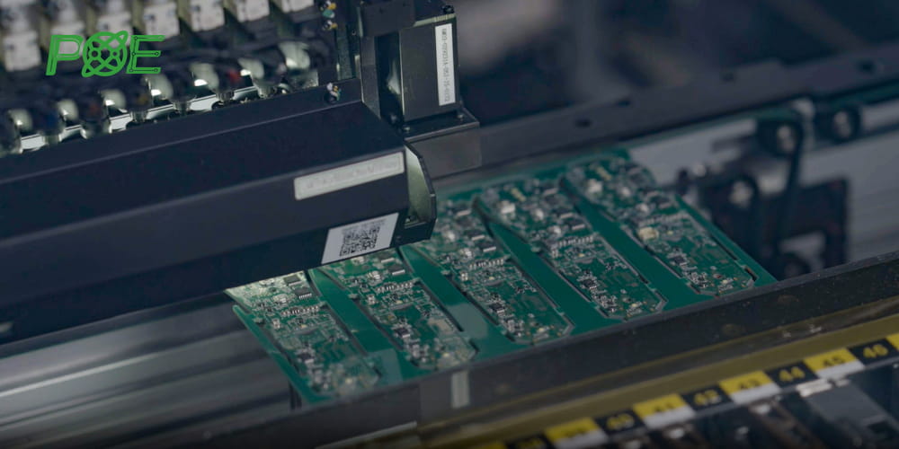
Our four Hanwha DECAN S1/S2 lines handle the heavy lifting. These machines use high-resolution vision systems to identify fiducials and place parts with micron-level accuracy. We routinely handle 01005 chip resistors and fine-pitch components down to 0.3mm pitch (BGA/QFN). At these scales, "eyeballing it" isn't an option—the machine either has the mechanical rigidity to hit the mark, or it doesn't. Our placement accuracy ensures that self-alignment during reflow works exactly as intended.
Step 3 – Reflow Soldering
The board enters a convection oven with precisely controlled thermal zones. We track the ramp-up, soak, reflow, and cooling phases obsessively. A stable thermal profile prevents component cracking (popcorning) and ensures proper intermetallic compound formation. This is where nitrogen atmosphere really pays off, minimizing voiding in BGA packages.
Step 4 – Inspection and Testing
We don't rely on visual sampling. Every single board goes through In-line AOI (Automated Optical Inspection). For components with hidden solder joints like BGAs, we run 2D X-Ray inspection to verify ball collapse and check for voids. Finally, we perform Functional Circuit Testing (FCT) to ensure the board performs to your specs in a real-world simulation.
SMT vs. Through-Hole
While SMT dominates, THT hasn't disappeared.
Dimension
SMT
Through-Hole (THT)
Component Size
Extremely small (01005)
Larger, bulkier
Circuit Density
Very High (Double-sided)
Low
Assembly Method
Fully Automated
Manual or Wave Solder
High-Volume Cost
Low
High
Mechanical Strength
Moderate
High (Vibration/Shock resistant)
High-Frequency Perf
Excellent
Limited by parasitics
Rework Difficulty
High
Lower
Use SMT for everything dense and digital. Use THT for connectors, large transformers, or anything subject to physical shear forces. Most modern designs use a hybrid approach—SMT for the brains, THT for the brawn.
What Determines SMT Assembly Quality?
1. DFM (Design for Manufacturability) Review
We don't just load your Gerbers and hit "Start." Our engineering team conducts a thorough DFM review beforeproduction. We look for insufficient annular rings, poor solder mask clearances, and component spacing issues. We provide actionable feedback—not just "this won't work," but "try this pad layout instead." We also suggest alternate components if your first choice creates a supply chain bottleneck.
2. Equipment Capability
Hardware sets the ceiling. With our DECAN S1/S2 lines, we aren't guessing if we can place your 0.3mm pitch QFN; we know we can. Our in-line AOI catches what the human eye misses at 20-micron resolutions.
3. Process Control
This is the "software." It's how we manage solder paste viscosity, how often we clean stencils, and how we optimize the reflow profile for your specific board(not just a generic setting). Our ESD-protected facilities and strict IPC-A-610 Class 3 compliance ensure consistency from the first board to the ten-thousandth.
4. Supply Chain Integrity
Defects often start with the parts. We leverage our supply chain network to ensure component authenticity and availability. In one recent case, our proactive sourcing strategy helped a client consolidate their BOM, reducing their total component procurement cost by 15% without sacrificing quality or lead times.
SMT Across Industries
Medical Devices: Our ISO 13485:2016 certification and IPC Class 3 standards ensure the reliability required for life-saving equipment.
Automotive & Industrial: We adhere to strict process controls to ensure zero-defect tolerances demanded by ADAS and industrial automation.
AI & High-Speed Computing: The short leads of SMDs are critical for maintaining signal integrity in high-speed backplanes and server motherboards.
General OEM: Full RoHS, REACH, and UL compliance across all assemblies.
How to Choose an SMT Assembly Partner?
Ask for Specifics: Don't ask "Can you do fine pitch?" Ask "What is your smallest stable pitch and what is your yield rate at 0.3mm?" (Ours is >99%).
Verify Certifications: Ensure they have the right certs for your industry (e.g., ISO 13485 for medical, IPC Class 3 for high-reliability).
Demand Engineering Support: Do they offer free DFM? Will they suggest cost-saving alternatives?
Check the Workflow: Is AOI 100% in-line? Is X-Ray available for BGAs? (It should be).
FAQs
What is surface mount PCB assembly?
It is a manufacturing process where components (SMDs) are mounted directly onto the surface of a printed circuit board, allowing for higher component density and automated assembly compared to through-hole methods.
What is the difference between SMT and through-hole?
SMT uses smaller components placed on the board surface, ideal for high-density and automated production. Through-hole uses leaded components inserted into drilled holes, offering superior mechanical strength for connectors and high-stress applications.
What are the main steps in the SMT assembly process?
The core steps are: 1. Solder Paste Printing, 2. Component Placement (Pick and Place), 3. Reflow Soldering, and 4. Inspection (AOI/X-Ray/FCT).
What is DFM and why does it matter for SMT assembly?
Design for Manufacturability (DFM) is a review process conducted before production to identify design features that might cause failures or increase costs. It is critical for preventing defects in high-density SMT layouts.
What components can be used in SMT assembly?
Almost any passive or active component, including 01005 resistors, 0.3mm pitch BGAs, QFNs, CSPs, and connectors designed for surface mounting.
Is SMT or through-hole better for my project?
Use SMT for the majority of your circuitry to save space and cost. Use Through-hole for components requiring high mechanical strength or high power dissipation. Many projects use both (hybrid technology).
How does SMT assembly reduce costs?
Through extreme automation (high CPH), reduced board real estate, lower material costs (smaller components), and improved electrical performance which reduces the need for signal conditioning components.
What is the minimum component size for SMT assembly?
At our facility, we routinely assemble 01005 chip components and fine-pitch BGAs down to 0.3mm.
POE can quickly provide you with PCB prototype/ small and medium-volume PCB/ PCBA manufacturing. Send your PCB files or BOM list to us and you will get a quote as soon as possible!

 Email: all@poe-pcba.com
 Whatsapp: 85292069596
 Tel: 0755-25312250/ +8613798543496
 Factory Address: Floor 3, Jinyuan Industrial Park, No. 56, Tangtou Avenue, Shiyan Town, Baoan District, Shenzhen China





