Solder Material and Equipments
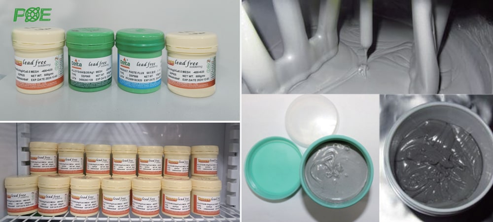
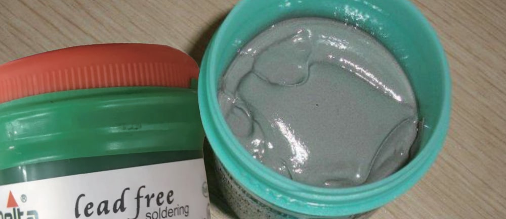
Solder Paste and Nitrogen ReflowSolder paste is an important material used in PCBA surface mount technology (SMT), which mainly consists of tin powder and flux. According to the market as well as our POE usage, we mainly introduce lead-free solder paste which is widely used nowadays.Introduction of Lead-free Solder Paste
Lead-free Solder Paste:
Lead-free solder paste is mainly composed of Sn-Ag-Cu (tin-silver-copper) alloy. Compared with traditional leaded solder paste, lead-free solder paste has significant advantages in terms of environmental performance, solderability and heat resistance.
Among them, the environmental performance of lead-free solder paste is one of the most important advantages. Since it does not contain the harmful metal element lead, lead-free solder can effectively reduce the emission of pollutants and protect the environment and human health.
In addition, lead-free solder paste has good solderability, good wettability and stability, and can meet the needs of high-speed connection of electronic components. Lead-free solder paste also has high heat resistance and remains stable when soldered at high temperatures.
Lead-free solder paste is widely used in electronic manufacturing, automobile manufacturing, medical and health care and other fields, especially in the consumer electronics manufacturing industry.
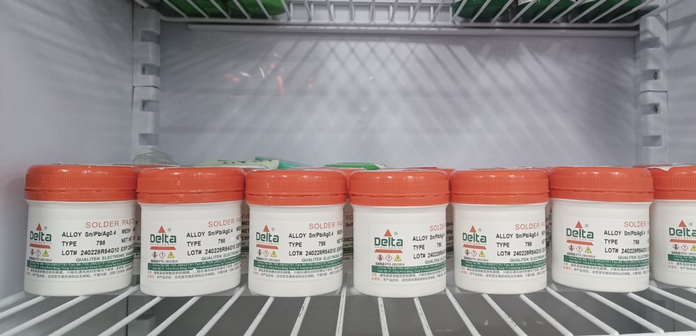
Accompanied by the national requirements for environmental protection, lead-free technology in the SMT processing industry will become a trend.POE Solder Paste Storage and Operation NormsIn the SMT production line, quality is the top priority, and this production of defective rate of 60%-70% is generated in the soldering process, most of the reasons are related to the use of solder paste and improper storage. POE adheres to the following norms during assembly process to ensure the quality of the solder as well as the product. (1) Before the solder paste is stored in the warehouse, it needs to be labeled with the date of purchase to distinguish different batches. We will control the use of solder paste cycle according to the SMT orders, since the inventory is generally controlled within 30 days. And solder paste storage should be placed separately according to different types, batch numbers, different manufacturers, solder paste should be stored in refrigeration after purchase, and should follow the principle of first-in-first-out.
(2) The solder paste is stored in the refrigerator, which is equipped with a special thermometer, and its storage temperature shall be controlled within the range of 2-10℃, and our POE staff will test the storage temperature every 12 hours and make a record.

(3) Take out of the refrigerator at least 4 hours prior to use and wait the solder paste to return to room temperature before opening the container to prevent condensation of water vapor and the formation of solder beads.

(4) After opening, we will use a mixer to make the ingredients in the solder paste uniform and reduce the viscosity of the paste.
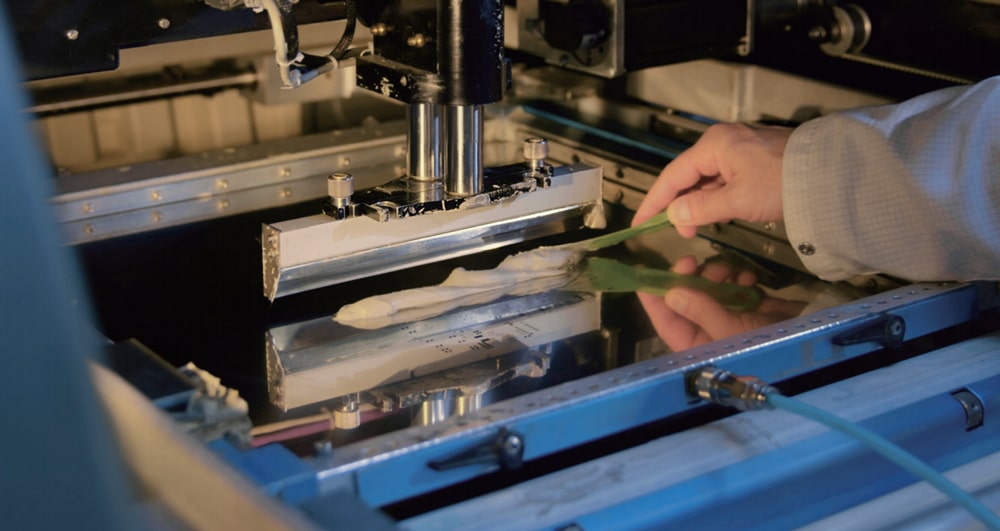
(5) Our staffs usually decide the thickness of solder paste according to the thickness of the stencil and the components on the PCB circuit board to ensure the printing quality. For example, there are stencil thickness specifications of 0.1mm, 0.12mm, 0.13mm, 0.15mm, 0.18mm, 0.2mm, etc. Usually, for a 0.12mm thick stencil, the thickness of the solder paste is usually controlled between 0.1mm-0.16mm.
(6) PCB board after printing solder paste should be posted in the shortest possible time to prevent flux paste and other solvents volatile. After printing failures, PCB bords should be required to be thoroughly cleaned and dried with ultrasonic cleaning equipment, in order to prevent the emergence of solder balls caused by residual solder paste after reflow soldering again.
(7) There is strict temperature control in our SMT production line. The optimal temperature for printing is 25C±3C, and the relative temperature should be 45%-65% . If the temperature is too high, the solder paste will easily absorb water vapor and produce solder beads during reflow soldering.
(8) After the solder paste printing machine, we will use SPI to carry out 10% inspection on the quality of the solder paste printing, it can effectively detect the printing volume, height, area, flatness and other defects of the solder paste, to ensure the quality of the printing and the final product. Nitrogen Reflow Soldering
Reflow soldering is a common technology in the electronics manufacturing industry, in which the solder paste on electronic components and printed circuit boards is melted by heating at high temperatures to bond them together.
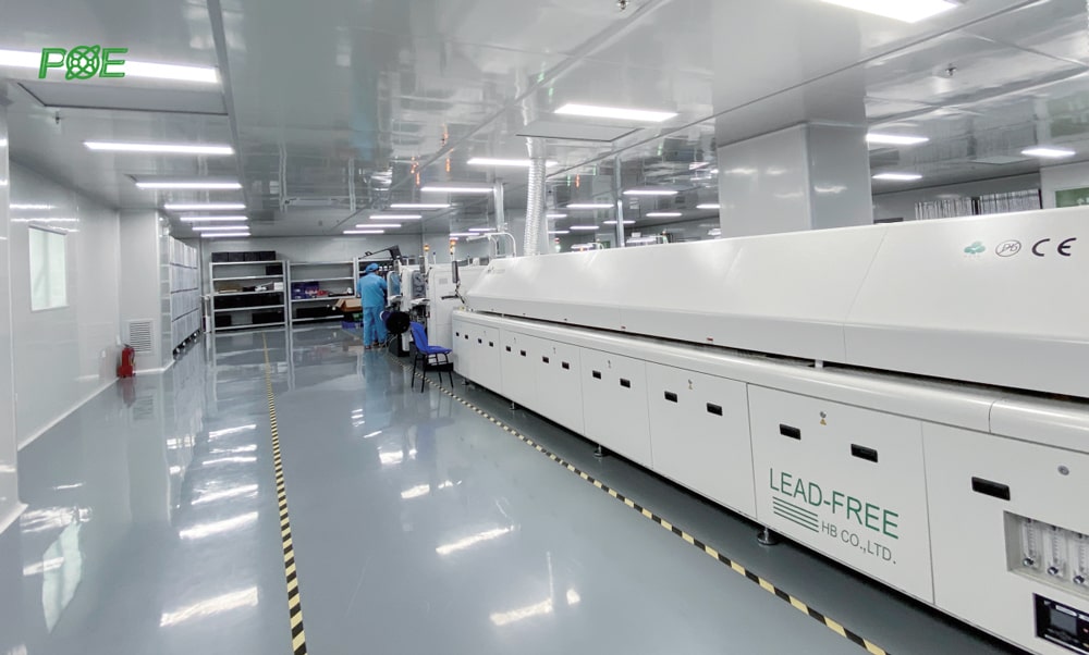
During the soldering process, oxygen may lead to oxides on the surface of the solder, affecting the quality of the solder joints and thus the reliability of the product. Nitrogen reflow soldering is a process of filling the reflow oven with nitrogen to reduce oxidation of the solder surface.
Nitrogen is a kind of inert gas, which is not easy to have a chemical reaction with the metal, isolate the oxygen in the air and electronic components contact, thus reducing the flux moisture volatilization in the reflow process. For products with high stability and reliability requirements, we are usually required to use nitrogen for soldering. Compared with normal reflow soldering, nitrogen reflow soldering can make the solder paste to play a better welding effect, increase the yield of the PCBA board, improve product quality and reduce the cost of rework or repair to a certain extent.
The surface tension of the solder paste under nitrogen is lower than when exposed to the atmosphere, which results in a significant improvement in the wetting and flow of the paste. Especially for fine-pitch components, the higher surface tension can reduce the incidence of bridging, as the solder will fuse once it melts, which may result in the solder returning to the pads, and also help to mitigate beads and other similar solder defects that are undesirable in the reflow process between chip components.
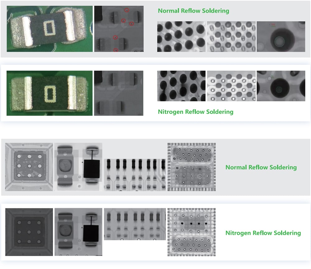
Comparison between Normal Reflow Soldering and Nitrogen Reflow Soldering: In addition, the nitrogen can significantly reduce the concentration of oxygen and materials that can contaminate the soldering surface, thus greatly reducing the oxidation of solder paste at high temperatures, especially for the reflow soldering quality enhancement of the second side. In the SMT production, when PCB in the first side of the reflow soldering, the second side of the circuit board surface treatment is actually experiencing the same high temperature at the same time. The surface treatment of the PCB will be destroyed due to high temperatures, especially the OSP. And the oxidation at high temperatures is also being carried out rapidly. After adding nitrogen, it can greatly reduce the oxidation degree of the second surface treatment of the reflow soldering during the first side of the reflow soldering, and has the best soldering effect.
 Nitrogen Reflow Soldering Advantages
Improvement of Soldering Quality: Nitrogen reflow soldering effectively reduces the generation of oxides, improves the wetting of solder joints, makes the surface of solder joints smoother and reduces defects.
Increase Reliability: Nitrogen reflow soldering reduces the oxygen content of the soldered area, helping to minimize the brittleness of the soldered interface and improve the long-term reliability of electronic assemblies.
 |
 |
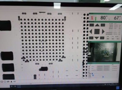
Regular Air Oven Soldering under X-Ray
Good quality
Good Stability
Recommend for high demand products |
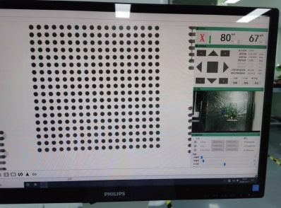
Nitrogen Oven Soldering under X-Ray
High Quality
High Stability
Recommend for high-end products |
Reduce Soldering Defects: Nitrogen reflow soldering significantly reduces common soldering defects such as short circuits, voided welds, solder balls, and cracks, increasing production yields.Application1.Products with high precision soldering needs, the use of nitrogen furnace will help reduce the defective rate.2.The boards with OSP surface treatment and double-sided reflow soldering are suitable for the use of nitrogen oven.3.The boards with large packages and high-density BGAs, as well as the boards with small components below 0201. 4.It can be applied when the effect of soldering of parts or boards is not good, such as to increase the wettability of QFN soldering.5.It is applicable to high-precision, high requirements of the semiconductor, aerospace, medical, automotive electronics, 5G communications, LED and other fields.
Solder Bars and Wave Soldering
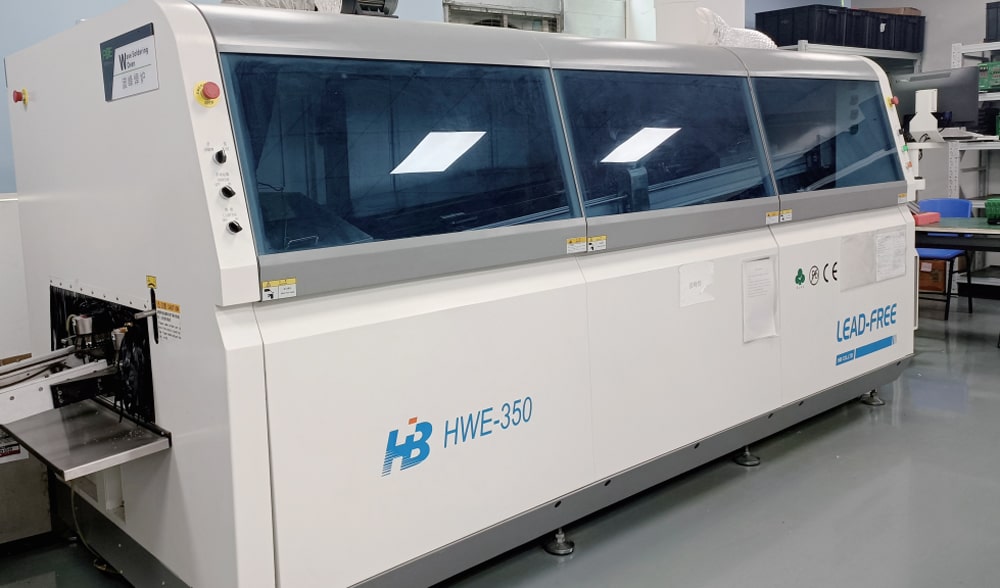
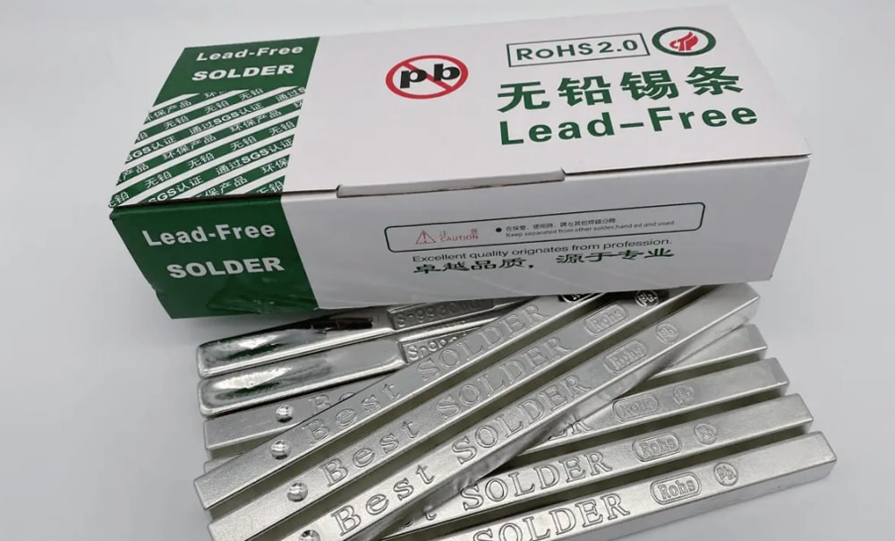
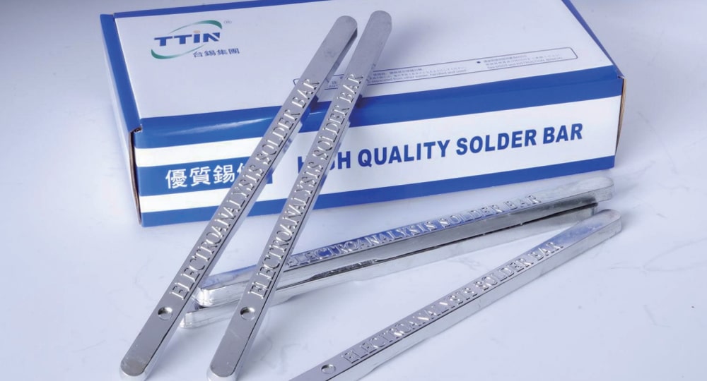
Wave SolderingWave soldering is a soldering method that connects electronic components to printed circuit boards. Its core principle is to use molten solder waves to solder components to the PCB. During the wave soldering process, the pads on the PCB are first coated with flux, and then the components are placed on the PCB. Next, the printed circuit board will be fed into the wave soldering machine via a conveyor belt. There is a molten solder wave inside the soldering machine. When the PCB passes through this wave, the solder will be adsorbed on the pads and component pins, forming solder joints to connect the components to the PCB. Finally, the printed circuit board enters the cooling zone for cooling, so that the solder joints solidify, completing the entire soldering process. Solder Bars - Wave SolderingThe solder for wave soldering is mainly tin bar, which is made of pure tin without adding flux. It is formed by melting pure tin directly, and there is less tin slag. When using tin bar for wave soldering, it should be used with flux. The molten liquid tin is soldered to the pads of the circuit board with components inserted, so that the component pins are soldered to the circuit board together, which meets the needs of wave soldering and improves the utilization rate.Characteristics of Solder Bars:1.Pure tin manufacturing, less slag, improve utilization, and has excellent antioxidant properties; 2. Low viscosity after melting, good fluidity, high solderability, most suitable for wave soldering process; 3. Due to minimal oxidation inclusions, it can minimize the phenomenon of tip pulling and bridge linking, reliable welding quality, and bright and full welded joints.Solder Bars:
 How do POE choose the right Solder Bar?Lead-free Solder Bar:Lead-free solder bars are composed of tin, copper and silver, which meet the strict requirements of the EU RoHS environmental protection directive, have higher performance, and components can withstand relatively high temperatures, it is the choice of most customers at present.
 Purity of the Solder Bar:A good solder bar can ensure uniform expansion during welding, thereby reducing the stress generated by soldering and improving the reliability of soldering. However, impurities in the tin bar will affect the quality and reliability of soldering, and may even cause problems such as short circuit or open circuit at the soldering point Generally speaking, a high-purity tin bar with a purity of more than 99.9% is the most ideal choice.
Liquidity of the Solder Bar:
During the wave soldering process, the solder bar needs to melt through high temperatures and form a good solder joint on the printed circuit board. If the fluidity of the solder bar is not enough, it will lead to uneven weld seams, air bubbles or other soldering problems.
The Melting Point of the Solder Bar:
The melting point of the solder bar should be lower than that of the solder joint so that it can melt and liquefy during soldering to form a good solder joint. If the melting point of the solder bar is too low, the temperature difference between the bar and the solder joint will be too large, thus affecting the quality and reliability of the solder joint. Therefore, when choosing the material of the solder bar, we pay attention to its melting point and the material matching of the solder joint.
Solder Bar Surface Quality:
Solder bar need to be melted to form liquid tin when soldering, therefore, oxides, grease, dirt and other impurities on the surface of the solder bar will affect the liquid tin's fluidity and wettability, thus affecting the quality and reliability of the solder joints. Therefore, the quality of the surface of the solder bar is very important. Generally speaking, solder bars need to be strictly cleaned and inspected during the production process to avoid surface contamination.

POE has Strict Specifications for the Packaging and Storage of Solder Bars:
Solder bar should be stored in a dry, cool and ventilated place, avoiding moisture, heat or direct sunlight to ensure the quality and stability of solder bar.

Wave Soldering has very Strict Requirements for Solider Bars:
A good solder bar can ensure the quality and reliability of the soldering, so we integrate different considerations in the PCBA production process to choose the appropriate solder bar to achieve high efficiency and high quality wave soldering assembly.
At the same time, POE will also focus on the storage and cleaning inspection of solder bars to ensure the quality and reliability of soldering.
