Our website use cookies to analyze website accesses and improve your online experience. By continuing browsing this website,you agree to our use of cookies and privacy policy.
Accept all cookies
Decline
This website uses cookies:
Our website use cookies to analyze website accesses and improve your online experience. By continuing browsing this website,you agree to our use of cookies and privacy policy.
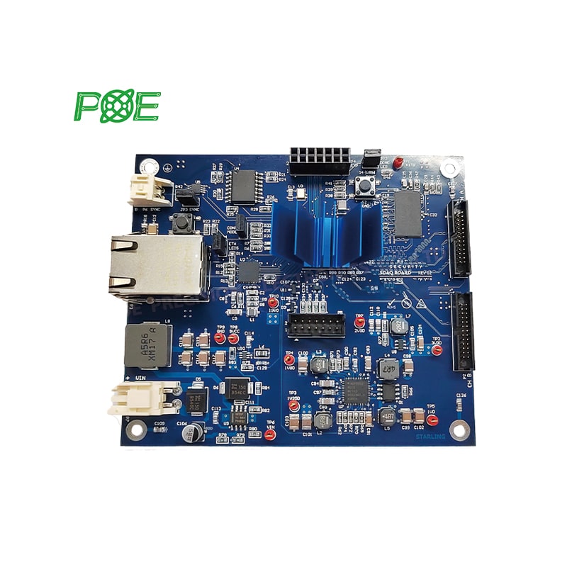
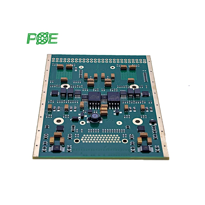
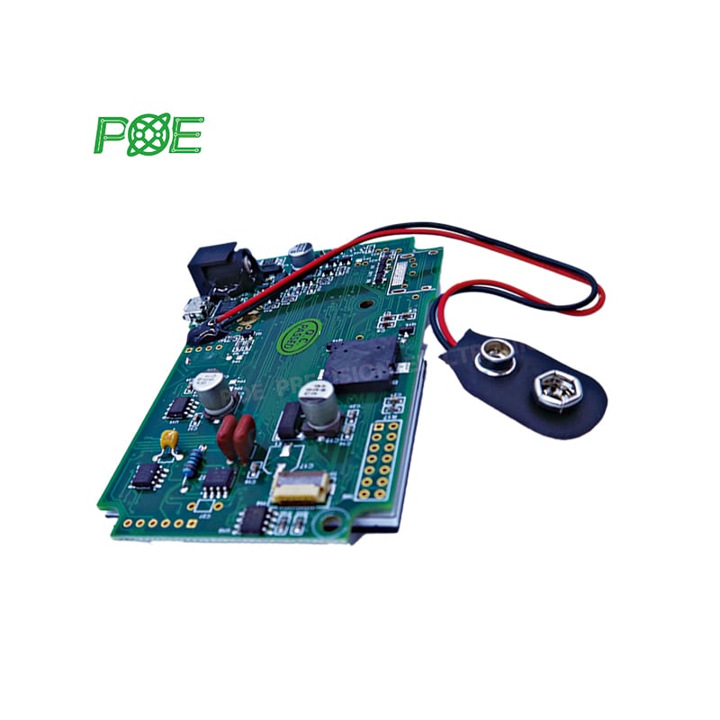
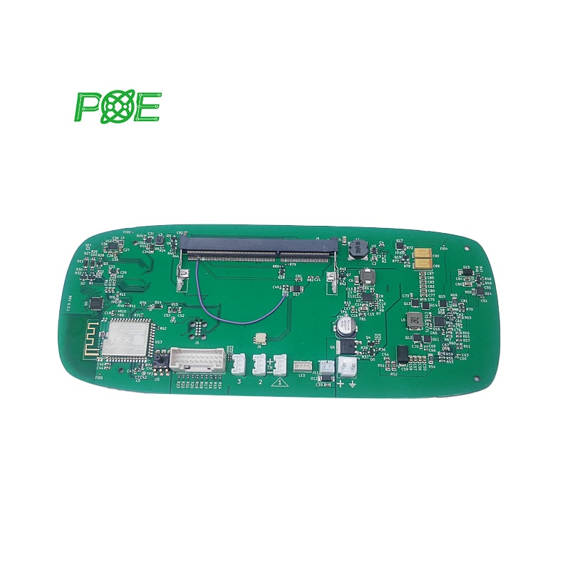
Electronic smart products in various fields are inseparable from PCBA with mature technology, and the complete PCBA process is composed of PCB manufacturing + PCB assembly.
What is PCBA?
PCBA is the abbreviation of Printed Circuit Board +Assembly. It is a bare PCB empty board that uses SMT and other processes to install components on the bare PCB board, and then goes through the process of DIP plug-in, which is called PCBA for short.
What is PCB?
Printed circuit board, referred to as PCB, is the support body of electronic components and the platform for electrical connection of electronic components.
There are also many materials used in PCB processing, such as PTFE (polytetrafluoroethylene), ROGERS ceramics, etc.
2. Classification of PCB
2.1 Material
Organic materials: phenolic resin, fiberglass/epoxy resin, Polyimide, BT/Epoxy, etc.
Inorganic materials: mainly based on their heat dissipation functions, such as aluminum, Copper-invar-copper, ceramic, etc.
2.2 Number of layers
Divided into single-panel SSB, double-panel DSB and multi-layer MLB. Common multi-layer boards are generally 4-layer boards or 6-layer boards, and complex multi-layer boards can have dozens of layers.
2.3 Soft and hard
Rigid circuit board RPC, flexible circuit board FPC, soft and hard combination PCB.
2.4 Single panel
This is the most basic PCB, with components concentrated on one side and wires concentrated on the other side. Because the wires only appear on one side, this type of PCB is called a single-sided PCB. Single-sided panels are rarely used now because the wiring cannot cross when designing circuits and must take separate paths.
2.5 Double panel
This kind of circuit board has wiring on both sides, and the lines on both sides are connected by vias. The area of a double-sided board is twice that of a single-sided board, and it can use intersecting wiring, so it can accommodate complex circuits. This is the most commonly used board today.
2.6 multilayer board
In order to increase the area that can be routed, multi-layer superposition technology is used to realize a four- and six-layer PCB that is more complex than a double-sided board, and can reach a maximum of more than 40 layers. The number of layers on the board represents several independent wiring layers, which is suitable for difficult projects.
Electronic components are inserted into the holes of the PCB. This method is suitable for small batches and proofing;
2.SMT
Electronic components are directly placed and pasted on the PCB surface, which is easier to automate. This method is suitable for medium and large-volume production and is currently the most commonly used method.
3.Mixed Technology
Some special components cannot be assembled using a single assembly technology. Flexible combination of the characteristics of the above two methods can achieve a balance between cost and mass production.
The above is the ultimate step-by-step guide to PCBA. A complete PCBA includes the process of PCB manufacturing, component procurement, and PCB assembly. Choosing an experienced PCBA manufacturer can advance your project progress and get your products to market faster! Contact us to start your PCBA manufacturing.
POE can quickly provide you with PCB prototype/ small and medium-volume PCB/ PCBA manufacturing. Send your PCB files or BOM list to us and you will get a quote as soon as possible!


 Email: all@poe-pcba.com
 Whatsapp: 85292069596
 Tel: 0755-25312250/ +8613798543496
 Factory Address: Floor 3, Jinyuan Industrial Park, No. 56, Tangtou Avenue, Shiyan Town, Baoan District, Shenzhen China