What is PCB Potting Process?
21 January 2025
Views: 3335
The PCB potting process is a method of protecting PCBA and is usually the last step in PCB assembly. The potted PCB circuit board can be waterproof, acid, alkali, dust, harsh environment (can adapt to -60-250℃), conductive pollutants, chemical erosion, vibration and impact, and improve electrical insulation and heat dissipation performance . Compared with conformal coating, the potting process is chosen to cope with harsher working environments.
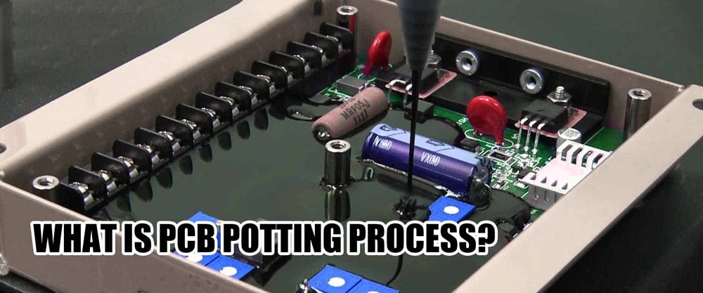
Common PCB potting adhesives include Silicone, Acrylic, Ester, Polyurethane, etc., which can be selected according to the requirements, such as cold, humid, high temperature and other different environments. Potting glue can be injection molded, coated, liquefied potting, spraying, etc. Different methods can achieve different effects and shapes. Before starting the PCB potting process, it is necessary to clean the PCBA to ensure that the potting glue can adhere perfectly.
The steps of PCB potting process are also very simple, mainly including the following steps:
1. Prepare the potting glue; 2. Mix the curing agent evenly. 3. Inject the mixed potting glue into the gaps of the PCBa; 4. Wait for the potting glue to dry, which usually takes about 24 hours to complete; 5. Carry out subsequent processing and testing of the PCBA normally.

The PCB potting process is a process used to protect PCBA products from operating normally in harsh environments. It can prevent PCBA from being affected by chemical substances and harsh environments. Compared with the conformal coating process, the thickness of the PCB potting process is increased several times, and the protection capability is also improved several times.
Share This Story, Choose Your Platform!

 Email: all@poe-pcba.com
 Whatsapp: 85292069596
 Tel: 0755-25312250/ +8613798543496
 Factory Address: Floor 3, Jinyuan Industrial Park, No. 56, Tangtou Avenue, Shiyan Town, Baoan District, Shenzhen China


