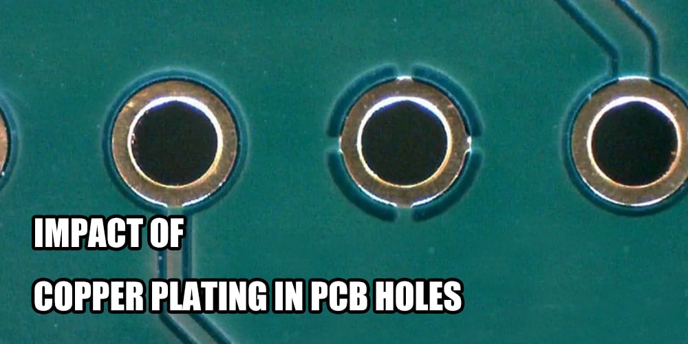
Impact of Copper Plating in PCB Holes
21 January 2025
Views: 3082
What is copper plating in PCB holes?
Copper plating refers to the copper deposited on the walls of the holes. After drilling is completed in a printed circuit board (PCB), there is no conductor inside the holes. Typically, copper is first deposited on the hole walls (as a conductor), and then it is further thickened to the required thickness through two electroplating processes.
The thickness of copper plating in the holes is one of the important factors that affect the reliability and lifespan of the PCB. When the plating is too thin, there is a possibility of the plated through hole being broken when subjected to high temperatures or large currents, resulting in the failure of the board. The thickness of copper plating in PCB holes is mainly determined according to IPCQ standards. These standards ensure the quality and performance of the PCB products. The copper plating thickness in PCB holes can be divided into three major classes:

Class 1 - General Electronic Products:
For general electronic products, the required minimum copper plating thickness in the holes is usually 20μm (micrometers). This is suitable for everyday electronic devices where reliability and lifespan are not critical factors.
Class 2 - Dedicated Service Electronic Products:
In products with higher requirements, such as communication equipment or industrial control systems, Class 2 specifications require an average copper plating thickness in the holes of >20μm. Compared to Class 1 PCBs, Class 2 PCBs have better performance and can be used in more demanding environments.
Class 3 - High-Reliability Electronic Products:
For aerospace, medical, military, and other electronic applications requiring the highest level of IPC standards, Class 3 specifications require a minimum copper plating thickness in the holes of 25μm. PCBs that meet Class 3 standards are designed to achieve optimal performance.
The thickness of copper plating in PCB holes has a significant impact on the performance of the circuit board. For example:
The copper plating thickness determines the ground resistance between the inner signal layers and the ground layer of the PCB, as well as the crosstalk between signal layers. If the copper plating thickness is small, the ground resistance increases, leading to increased signal noise. At the same time, crosstalk is intensified, affecting signal integrity.
If the copper plating thickness in the holes is too thin, the hole walls become fragile and prone to fracture. On the other hand, if the copper plating thickness is too thick, it affects the hole's fit and perforation performance, thereby impacting inter-board reliability.
A thin copper plating in the holes may cause solder pads to peel off easily. Conversely, if the copper plating thickness is too thick, it affects the temperature and time required for soldering, thereby affecting the quality of the solder joint.
Depending on the design and performance requirements, different copper plating thicknesses in the holes may be needed. Choosing the appropriate copper plating thickness allows the product to achieve the best balance between cost and performance.
If you have any needs, please contact us. The PCB products we provide to our customers use 25μm or more hole copper to ensure product quality.

Email: all@poe-pcba.com
Share This Story, Choose Your Platform!

