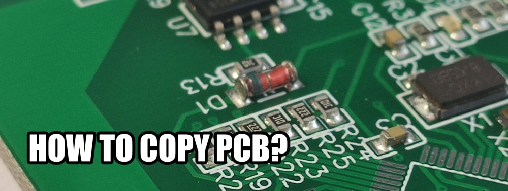
How to copy PCB board?
BOM single production and disassembly
In PCB board cloning, the production of BOM list is a key link. The subsequent procurement of components, various functional modules of the PCB board, and the final welding and debugging of the PCB clone board all rely on this file. Because this list includes the relevant parameters and specifications of all components on the PCB, it is an important part of board copying and design.
In the production of BOM list, the contents that need to be clearly marked include component name, component specification, component position number, component material number, component material specification, component shape and shape code, etc. BOM list preparation steps:
1. Preparation
First get a PCB, take two photos of the location of the vitality parts with a digital camera, and pay attention to the shooting effect. Record the model, parameters, and location of all vitality components on paper, especially the direction of the diode, triode, and IC notch.
2. Dismantling records
Remove all components one by one. When disassembling the board, the intact original board will be split into bare boards and components. It is important to prepare the BOM list during the disassembly process. Professional board dismantling personnel will prepare a piece of white paper and a pen before copying the board, and first write down the serial number and the position number of the components on the paper. After each component is removed, the corresponding position number is Use double-sided tape to stick it on white paper. It should be noted that during the process of splitting the board, special care must be taken in the arrangement of component numbers, because an error in the location information of one component may lead to inaccuracy in the entire BOM list, affecting the cloning effect.
3. Component testing
After getting the sequence list recording component information from the board dismantling personnel, they officially enter the BOM production process, which is the process of summarizing all relevant parameters of the components into an information table through testing and analysis.
4. Make a BOM list and inspect it
The criterion for judging the accuracy of the BOM list is to combine various test data and component models, parameters, specifications, etc. into a table to form the BOM list.
5. Material procurement
The impact of BOM production efficiency on subsequent production The BOM list is the main basis for component procurement and the material basis for subsequent product production. Therefore, its production efficiency will have an important impact on subsequent processes.
scanning
Use a scanner to scan in the images of each layer of the printing plate and convert them into an image format that can be accepted by conversion software such as BMPTOPCB and QUICKPCB. The image format is generally BMP format. Note that the PCB must be placed horizontally and vertically in the scanner, otherwise the scanned image cannot be synthesized by PROTEL and the file cannot be saved. Steps: Remove the tin from the PAD hole. Clean the PCB with alcohol, and then put it into the scanner. When the scanner scans, you need to slightly increase the scanning pixels in order to get a clearer image. Start POHTOSHOF and scan the silk screen surface in color, save the file and Print it out for later use. Use water gauze paper to lightly polish the TOP LAYER and BOTTOM LAYE layers until the copper film shines. Place it in the scanner, start PHOTOSHOP and scan the two layers in color. The fourth step is to adjust the contrast and lightness of the canvas so that the part with copper film and the part without copper film have a strong contrast. Then convert the image to black and white and check whether the lines are clear. If not, repeat this step. If it is clear, save the image as black and white BMP format files TOP.BMP and BOT.BMP. If you find problems with the graphics, you can use PHOTOSHO P to repair and correct them. Convert the two BMP format files to PROTEK format files, and transfer the two layers in PROTEL. If the positions of PAD and VIA after the two layers basically coincide, it indicates that the first few steps have been done well. If there is a deviation, then Repeat the scan.
PROTEL synthesis
Open the AUTO CAD software, create a new CAD file, and select Insert bitmap image in the Insert menu. After selecting the image you want to insert, the Insert Image dialog box will appear. In the dialog box, select the ratio of 1:1. Insert PCB image. Draw a rectangular frame to cover the border of the PCB diagram. Note that when drawing the border, you must use the object tracking object lock point. If you do not draw a border, the image will move accidentally during the process of drawing the circuit diagram and it will be difficult to register. up•
Draw the component footprint. The component package used in the PCB board to be copied may not necessarily match the component package in PORTEL 99, so we have to create the component package ourselves. First, count how many packages are used on the PCB board. Only one of each package needs to be drawn. After all the packages are painted, they must be transferred to PORTEL 99 for further processing.
Open PORTEL99, first create a new PCB file, select Import CAD file in the file menu of PORTEL 99 PCB editor, and import the CAD file with the drawn component model. After the import is successful, the component package will appear in PORTEL 99 PCB editor. Basic graphics. Modify appropriately in PROTEL. After all component packages are produced, these packages are placed in the PORTEL99 PCB editor, and then exported as a CAD file. After opening the CAD file of the component package diagram, the previously imported PCB image The CAD file is also opened, and the component package diagram is copied to the CAD with the PCB picture. At this time, the CAD file with only the component package diagram can be closed. You only need to work in the CAD file with the PCB picture, and arrange the components according to the PCB picture. Place the angle and position, arrange the components one by one, and pay attention to using the copy and paste method to make more sub-components to place pads and vias. After placing the component package, the next step is to place the pads and vias. First measure the inner and outer diameters of the pads in CAD, then select the ring sub-item in the drawing menu and determine the inner and outer diameters of the ring. Outer diameter, when placing the pads, all pads of the same size must be placed at once. However, square pads and polygonal pads cannot be placed. Although polygons can be filled into entities using the filling method in CAD, but filling After the entity is transferred to PORTEL 99, there will only be an empty border. Therefore, if there are polygonal pads in the PCB diagram, we can use lines to trace the edges of the pads, transfer to PORTEL 99, and then put the corresponding pad .
Check
Use a laser printer to print the TOPLAYER BOTTOMLAYEF onto transparent film (1:1 ratio), and put the film on the PCB for comparison. If there are no defects, it is successful.

 Email: all@poe-pcba.com
 Whatsapp: 85292069596
 Tel: 0755-25312250/ +8613798543496
 Factory Address: Floor 3, Jinyuan Industrial Park, No. 56, Tangtou Avenue, Shiyan Town, Baoan District, Shenzhen China


