In the SMT era, "solder side" has largely been replaced by "secondary side." At POE, when we review customer files, we now assume double-sided placement unless the BOM or enclosure explicitly rules it out. Mobile and IoT designs, for instance, routinely rely on double-sided boards to position decoupling capacitors as close as possible to fine-pitch BGA pads—something a single-sided layout simply cannot do without sacrificing board area or signal integrity.
Single-Sided vs. Double-Sided
| Dimension |
Single-Sided |
Double-Sided |
| Component Placement |
One side only |
Both sides |
| Available Area |
100% of board surface |
Up to ~200% theoretically; ~150–180% practical after clearances |
| Circuit Density |
Lower |
Significantly higher—often 40–60% more components in the same footprint |
| Design Flexibility |
Limited |
High—analog/digital, RF/baseband can be separated |
| Board Size |
Larger for same functionality |
Smaller—critical for space-constrained products |
| Manufacturing Complexity |
Lower |
Higher—two reflow passes required |
| Cost |
Lower per board |
~25–35% higher than single-sided |
| Common Applications |
Simple controls, LED boards |
Consumer, automotive, medical, telecom, industrial |
Single-sided makes sense for low-density, cost-first designs where space is not constrained. For almost everything else, double-sided is not an upgrade—it is the baseline.
The Double-Sided Assembly Process
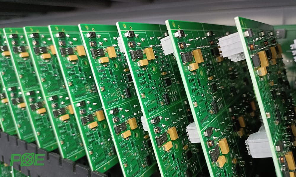
Solder Paste Printing (Side A) – Stencil printing on the first side.
Component Placement (Side A) – Pick-and-place for SMDs.
Reflow Soldering (Side A) – First reflow pass.
Inspection (Side A) – AOI verification.
Flip Board – Expose the secondary side.
Solder Paste Printing (Side B) – Second-side stencil printing.
Component Placement (Side B) – Placement on the secondary side.
Reflow Soldering (Side B) – Second reflow pass.
Final Inspection – AOI, X-ray (for BGAs), and functional testing.
The A/B Flip Panel Technique
One detail that often surprises procurement teams: we can process both sides using a single stencil and a single pick-and-place program. In an A/B flip panel, half the boards are oriented topside-up, the other half upside-down and rotated 180°. From a machine perspective, the panel looks identical from either side. This reduces setup time and keeps line balance even when one side carries significantly more components than the other—a small optimization that can shave hours off lead time on medium-to-high mix orders.
Two Reflow Passes and What They Mean
The defining technical reality of double-sided assembly is simple: components on the first side go through reflow twice. The second pass re-melts the first-side solder if you let it—and gravity does not need an invitation.
Why Components Usually Stay Put
In practice, most first-side components survive the second reflow without issue, thanks to three physical effects we design around every day at POE:
Melting point shift: Lead-free alloys like SAC305 start at 217°C. After the first reflow, microstructural changes raise the effective melting point to ~220°C or higher, making re-melting less likely.
Surface tension: Molten solder cradles small, light parts. For 0201/0402 passives, surface tension easily overcomes gravity during the second pass.
Oxide layer formation: A thin oxide skin forms after the first reflow, adding mechanical stability.The Practical Rule We Use
Heavy components go on the side soldered last. Connectors, large BGAs, transformers, and shielded modules belong on the secondary side whenever possible.
Keep the first side light. Resistors, capacitors, and small ICs are ideal for the first pass.
Adhesives, but sparingly. If a heavy part must be on the first side, epoxy under the component can help—but it complicates rework and adds cost. We typically treat this as a last resort rather than standard practice.
This rule sounds simple. In our experience, most field failures traced back to double-sided assemblies come down to ignoring it.
Double-Sided BGA Assembly
Double-sided BGA placement is where performance meets process risk. It allows maximum component density—essential for smartphones, advanced driver-assistance systems (ADAS), and compact medical devices—but it also compresses your margin for error.
Thermal stress and warpage: Multiple reflow cycles can cause low-Tg substrates to bow. Even a few hundred microns of warpage can compromise BGA solder joints.
Solder joint reliability: Large BGAs are prone to cracked joints during the second reflow due to board flex and flux depletion.
Inspection complexity: When BGAs overlap through the board, X-ray images can obscure each other. We address this with angled X-ray shots and, when necessary, laminography.
Rework difficulty: Access is limited once both sides are populated. Designing in test points and keeping critical nodes accessible pays off later.
From a routing standpoint:
Non-overlapping BGAs allow conventional through-holes.
Partially overlapping BGAs require blind or buried vias in the overlap region—an added cost, but often unavoidable in high-density layouts.
What Double-Sided Assembly Actually Costs
Typical cost drivers include:
An additional reflow pass
Additional pick-and-place time
Setup fees for each side (commonly in the $20–$30 range per side)
Potential fixturing or adhesive costs
As a rough benchmark, double-sided PCB assembly is usually 25–35% more expensive than a comparable single-sided build. But that number only makes sense in context.
Example scenario:
A mid-complexity IoT controller with 350 components:
Single-sided: 100 × 80 mm board, simpler routing, lower assembly cost per board.
Double-sided: 80 × 65 mm board, same functionality, ~30% higher assembly cost per board.
The double-sided version may cost more per board, but it reduces:
Enclosure size and tooling
Shipping weight and volume
Number of boards per system
Certification and compliance overhead
When we walk through TCO (total cost of ownership) with customers at POE, the double-sided option often wins—not because it is cheaper per board, but because it is cheaper per device.
Double-Sided vs. Multilayer
| Attribute |
Double-Sided |
Multilayer |
| Conductive Layers |
2 (top and bottom) |
3 or more |
| Substrate Layers |
1 |
Multiple, laminated together |
| Routing Complexity |
Moderate |
High |
| Cost |
Moderate |
Significantly higher |
| Lead Time |
Shorter |
Longer |
| EMI Performance |
Good |
Better (up to ~20 dB improvement possible) |
| When to Choose |
Most consumer, industrial, automotive applications |
High-speed digital, RF, dense routing requirements |
Applications
Consumer Electronics: Smartphones, wearables, and wireless earbuds depend on double-sided assembly to hit aggressive size targets.
Automotive Electronics: ADAS modules, ECUs, and sensor boards use double-sided layouts to fit into tight mechanical envelopes under the hood or behind panels.
Medical Devices: Implantable electronics and portable diagnostic equipment rely on the compactness and reliability double-sided assembly provides.
Industrial Electronics: Power supplies, motor drives, and control units benefit from higher density and better thermal distribution.
Telecommunications: RF modules and network hardware leverage double-sided designs for shorter signal paths and cleaner layouts.
What to Look for in a Double-Sided PCB Assembly Partner
Reflow process control: Can they document separate reflow profiles for Side A and Side B? How do they monitor first-side joint integrity during the second pass?
Component handling capability: Can they reliably place 0201/01005 passives and fine-pitch BGAs on both sides?
Inspection capability: Do they have AOI on both sides and X-ray for BGA inspection? Can they handle overlapping BGAs?
Fixturing and adhesive experience: Do they use custom carriers or pallets for secondary-side soldering? Under what conditions do they recommend adhesives?
Design for Assembly support: Will they review your placement strategy before production? Do they provide DFM feedback specific to double-sided constraints?
Quality system: Which IPC standards do they follow (e.g., IPC-A-610, IPC-6012)? What is their typical defect rate on double-sided builds?
At POE, we view these not as checklist items, but as the minimum baseline for any serious double-sided assembly program.
FAQ
Q: What is double-sided PCB assembly?
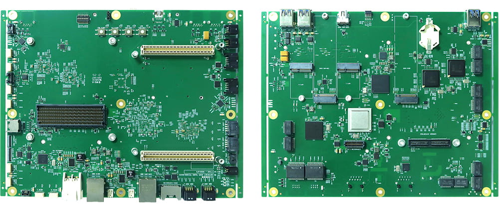
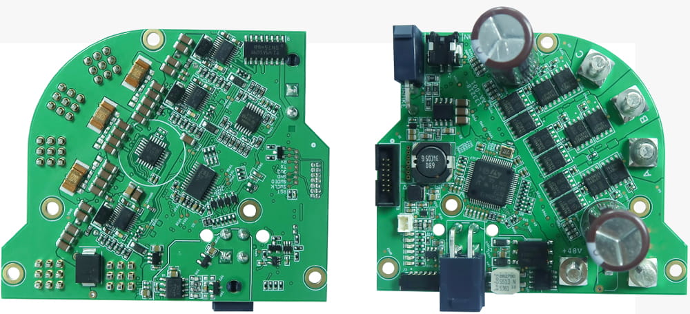
It is the process of assembling components on both the top and bottom surfaces of a PCB, effectively doubling usable component area without increasing board size.
Q: How is it different from single-sided assembly?
Single-sided uses one side only. Double-sided uses both, enabling higher density, smaller boards, and greater design flexibility—at the cost of additional process steps.
Q: What is the main technical challenge?
Preventing first-side components from detaching during the second reflow pass. This is managed through component placement strategy, thermal profiling, and material selection.
Q: Is double-sided assembly more expensive?
Yes—typically 25–35% more than single-sided—due to extra reflow, setup, and potential fixturing. However, total system cost often decreases.
Q: Can I place BGAs on both sides?
Yes, but it requires careful planning around thermal management, inspection, and routing. Overlapping BGAs add complexity and should be reviewed during DFM.
Q: What is the difference between double-sided and multilayer PCBs?
Double-sided refers to component placement on both outer layers. Multilayer refers to having three or more conductive layers laminated together. Many double-sided boards are also multilayer.
Q: What components should go on which side?
Place heavier components (connectors, large BGAs) on the side soldered last. Keep the first-pass side for lighter components such as resistors, capacitors, and small ICs.
Q: How do you prevent components from falling off during the second reflow?
By controlling component placement, optimizing reflow profiles, selecting appropriate board materials, and—only when necessary—using adhesives.

 Email: all@poe-pcba.com
 Whatsapp: 85292069596
 Tel: 0755-25312250/ +8613798543496
 Factory Address: Floor 3, Jinyuan Industrial Park, No. 56, Tangtou Avenue, Shiyan Town, Baoan District, Shenzhen China





