Bare PCB Introduction and Testing
21 January 2025
Views: 2950
1.What is a bare pcb?
1.What is a bare PCB?
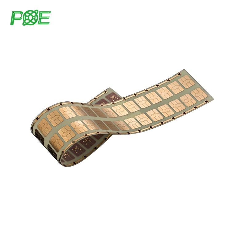
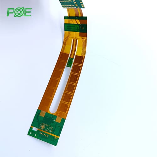
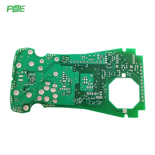
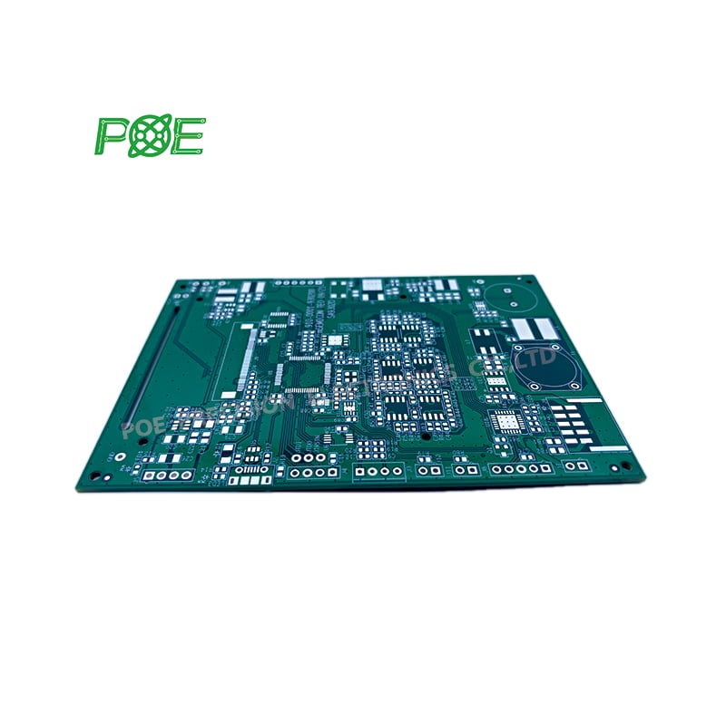
Bare PCB board refers to a printed circuit board without any through holes or components added. The industry is accustomed to calling it PCB, and the printed circuit board with components assembled is called PCBA in the industry. Bare PCB has only the most basic channels, patterns, metal coating, and substrate.

2.What is the role of bare PCB?
The first thing that needs to be confirmed is that the bare PCB will only be effective after adding components. Bare PCB is equivalent to the skeleton of a circuit board. The purpose of manufacturing is to add components and eventually become a complete circuit board. Different components can be assembled according to the design and applied to different application fields, such as medical, industrial, aerospace, etc.
3.What documents are needed to manufacture a bare PCB?
First, use PCB design software, such as Altium Designer, Eagle, kicad, etc. Generate Gerber drawing file format for manufacturing PCB. The Gerber file contains the outline, copper wire, pad, drilling, surface bonding line layer and other files needed to manufacture the bare PCB.

4.What is the process for manufacturing a bare PCB?
After receiving the documents from the customer, the bare PCB manufacturing process needs to go through the following 22 steps from raw materials to being sent to the customer:
1.Board cutting; 2.Drill; 3.Laser drill 4.Membrane pasting; 5.Circuit exposure; 6.Etch, developing; 7.Inner layer AOI; 8.Inner circuit Xray; 9.Lamination; 10.Copper plating+ VCP plating process; 11.D/F (Dry Film); 12.Outer layer Developing; 13.Pattern Plating; 14.Outer layer etching; 15.Solder Mask & Drying; 16.Legend; 17.Gold plating; 18.Milling ; 19.Sheets cutting; 20.Probe-flying test for prototypes; 21. E-TEST for mass production; 22.Packing &shipping.
5.Why bare PCB testing?
Bare PCB is the best time to test before completing the complete circuit board. Any subsequent problems that may arise will be avoided during testing at this time. Although the chance is very small, before proceeding to the next step of assembling components, the bare PCB may have some defects due to errors during manufacturing. For example: over-etching, under-etching, and holes. If testing is not performed after the bare PCB is manufactured, subsequent testing will become more complicated due to the increase in components. Once a fault occurs, repair will be very difficult.
6.What are the types of bare board testing?
6.1 Probe-flying test for prototypes
Flying probe test - Connect the software program to an automatic probe to test the connection of the bare PCB. Flying probe test takes longer than E-test, but the cost is low. It is very simple and easy to test bare boards of different designs. Suitable for proofing.

6.2 E-Test for mass production
Bare PCBs with larger sizes are tested this way using fixed fixtures, and the test is very efficient and can be completed in just a few seconds. However, the cost is higher, and different bare PCBs require different fixtures and pins, so they are very suitable for mass production product testing.

7.Conclusion
A bare PCB refers to a printed circuit board without adding any through holes or components. It is the basis for a fully functional circuit board. During the manufacturing stage of the bare PCB, the bare PCB needs to be inspected to prevent more errors during subsequent assembly.

 Email: all@poe-pcba.com
 Whatsapp: 85292069596
 Tel: 0755-25312250/ +8613798543496
 Factory Address: Floor 3, Jinyuan Industrial Park, No. 56, Tangtou Avenue, Shiyan Town, Baoan District, Shenzhen China