Base Material Properties and Microvia Reliability
The drive toward higher circuit density is challenging PCB manufacturers and their supply chains alike, with base materials as a critical foundation for complex designs. HDI designs present specific challenges and requirements for these materials, but given the myriad possible designs and applications, there is no optimal “one size fits all” material. Perhaps the most challenging HDI designs are those that use stacked vs. staggered microvias, with the number of layers of stacked microvias and the pitch between them as critical variables.
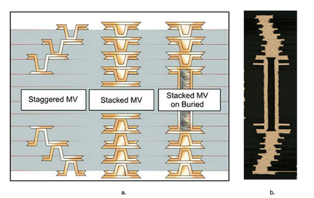
Figure 1: a) Illustration of staggered vs. stacked microvias; b) Seven stacked microvias on a buried multilayer sub-PCB.
Staggered microvias are offset on adjacent layers with separate drill axes. They distribute mechanical stresses more evenly across a larger area and, therefore, are generally more reliable. Stacked microvia designs enable more dense circuit routing but carry higher reliability risks under thermal cycling.
Staggered designs offer better durability at the cost of board real estate, whereas stacked microvias, with an increasing number of layers, are required for high-performance applications, including AI, high-performance computing, and networking equipment. While PCB drilling and plating processes are critical to microvia reliability, base material properties will also determine whether these structures survive assembly processes and field operation for the expected service lifetime.
As a PCB undergoes thermal cycling, first with exposure to high temperatures in reflow assembly processes, and then in the operating environment, these microvias are subjected to various thermomechanical stresses. The actual level of these stresses will be affected by the specific PCB design features, including the number of layers of microvias, the individual dielectric thicknesses and resin contents, as well as the geometries of the microvias, including whether staggered or stacked. A few types of microvia defects related to material properties are shown in Figure 2.
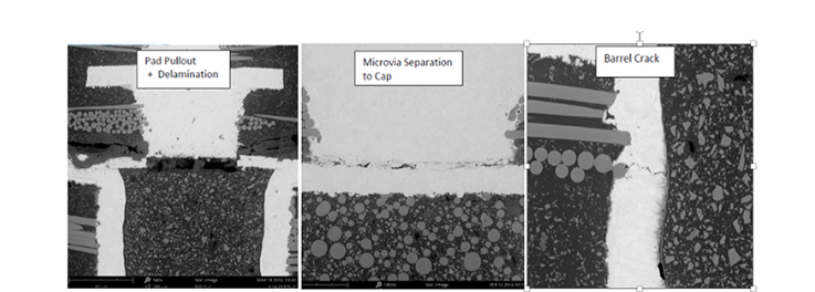
Figure 2: Examples of microvia defects.
From a base material perspective, there are a few critical properties to consider.
Thermal Expansion Properties
Glass-reinforced thermoset laminate and prepreg materials will have different CTEs in the X-Y and Z directions. While X-Y CTEs are important, especially when considering large-format component packages, for microvia reliability, Z-axis thermal expansion is most critical.
Share This Story, Choose Your Platform!

 Email: all@poe-pcba.com
 Whatsapp: 85292069596
 Tel: 0755-25312250/ +8613798543496
 Factory Address: Floor 3, Jinyuan Industrial Park, No. 56, Tangtou Avenue, Shiyan Town, Baoan District, Shenzhen China





