What is a PCB pad?
PCB pads are conductive areas (usually made of copper) on a PCB board for component mounting and electrical connections. They come in a variety of shapes and sizes, each with a specific purpose in electronic assembly. The main functions are to provide electrical connections, improve heat dissipation, provide solder joints, and align and position for automated assembly.
Types of PCB Pads
PCB pads can be classified based on shape, purpose, and location. There are three main types of PCB pads: surface mount pads, through-hole pads, and via pads. Each type has a specific purpose in PCB design and manufacturing.
1.Surface Mount Pads
Surface mount pads are flat metal areas on the PCB surface designed for surface mount technology (SMT) components. These pads allow components to be soldered directly to the PCB without drilling holes. The size and shape of SMT pads depend on the type of package the component is in, such as SOT, QFP, or BGA. Surface mount pads have solder mask openings that are slightly smaller than the copper area to prevent solder bridging.
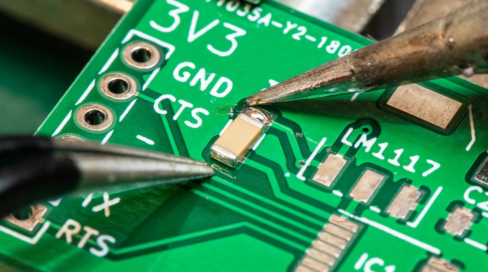
SMT pads save space and reduce PCB weight, allowing for higher component density. They are commonly used for resistors, capacitors, integrated circuits (ICs), and other small components.
2. Through-hole pads
Through-hole pads are copper annular rings surrounding plated through holes. They are used for through-hole component (THT) mounting, where component leads pass through the PCB and are soldered on the other side.
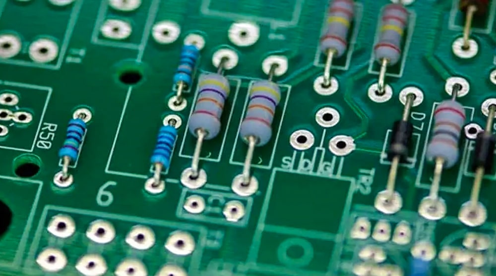
Copper-plated through-hole pads (PTH): PTHs have copper-plated walls that enable electrical connections between multi-layer PCBs.
Non-plated through-hole pads (NPTH): NPTHs are mounted with screws and do not provide electrical connections.
3. Via pads
Vias are a special type of pad used to facilitate electrical connections between different layers of a PCB. Unlike standard through-hole pads, vias are smaller in size and are not used for component mounting. There are three types of via pads:
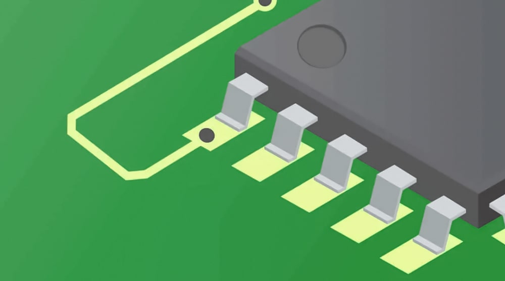
Blind vias: connect outer and inner layers.
Buried vias: connect inner layers but do not touch outer layers.
Through hole: penetrates all PCB layers and provides vertical connection.
Conclusion
The main function of PCB pads is to provide electrical connection, improve heat dissipation, provide soldering points, and provide automatic assembly alignment and positioning. PCB pads are divided into three types: surface mount pads, through-hole pads, and via pads.

 Email: all@poe-pcba.com
 Whatsapp: 85292069596
 Tel: 0755-25312250/ +8613798543496
 Factory Address: Floor 3, Jinyuan Industrial Park, No. 56, Tangtou Avenue, Shiyan Town, Baoan District, Shenzhen China


