In today's era of rapid technological development, the emergence of HDI PCB has completely changed the electronic world, allowing electronic devices to break through the boundaries of miniaturization without affecting performance.

What is HDI?
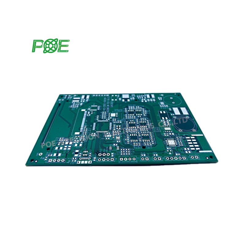
High Density Interconnect (HDI) PCB is a manufacturing technology used for printed circuit boards (PCBs) in electronics. HDI can achieve higher line density and smaller size, thus providing more functions and performance in a limited space. HDI utilizes microvias, blind and buried vias to create connections between different layers within a board, enabling designers to maximize component density while minimizing overall device size and weight.
Importance of HDI PCBs

1.Miniaturization of electronic equipment
HDI PCB technology contributes to a significant level of miniaturization in modern electronic devices, HDI PCB is able to support higher density components in a limited space, thus enabling sleek and compact designs without compromising performance. This enables the development of smaller, lighter, and more portable electronic devices.
2.Enhance signal integrity and reduce electromagnetic interference
Signal integrity is key to electronic devices, and HDI PCBs excel at ensuring reliable signal transmission by minimizing signal loss, crosstalk, and noise interference. Shorter distances between components and optimization of routing paths improve impedance control and minimize electromagnetic emissions. This not only improves overall performance, but also reduces the risk of potential failures.
3.Facilitate high-speed data transmission
HDI technology shortens interconnect lengths, reduces transmission delays, and enables high-speed data transmission within electronic devices. Additionally, the use of advanced materials with low dielectric constants can increase signal propagation speed while minimizing signal attenuation, enabling seamless communication between components.
Types of HDI PCBs

1.Sequential Build-Up (SBU) HDI PCBs
When it comes to accommodating moderate density interconnections, Sequential Build-Up (SBU) HDI PCBs prove to be a reliable choice. This type of HDI PCB design entails a sequential layer build-up process, wherein multiple layers are added one after another. The sequential approach allows for increased complexity and densification in electronic devices.
 HDI PCBs")
Due to their construction method, SBU HDI PCBs enable engineers to incorporate more components and interconnects into a smaller footprint. This makes them particularly well-suited for devices such as smartphones, tablets, and wearables where space optimization is critical.
By stacking the layers sequentially, these PCBs can achieve the desired density without compromising signal integrity or performance. SBU HDI PCBs serve as an effective solution for applications that require moderate density interconnections while ensuring efficient use of limited space and maintaining high functionality.
2.Stacked Via (SV) HDI PCBs
In the quest for achieving higher density interconnections within compact electronic devices with limited routing space, Stacked Via (SV) HDI PCB technology emerges as a game-changer. This type of HDI design employs stacked microvias to enable greater circuit density without sacrificing performance or reliability.
 HDI PCBs")
The key feature that distinguishes SV HDI PCBs is the utilization of microvias stacked on top of each other vertically, allowing for multiple connection layers in a single via footprint. By leveraging innovative manufacturing techniques and precision drilling processes, SV HDI PCBs can achieve impressive interconnect densities even in extremely small form factors.
The stacking nature of the vias provides designers with more room for routing traces on inner layers while maintaining the necessary connectivity between different components. This flexibility not only contributes to improved signal integrity but also enables efficient thermal management and better overall device performance.
3.Any Layer (AL) HDI PCBs
For those seeking the utmost design flexibility and the highest interconnect density in advanced electronic devices, Any Layer (AL) HDI PCBs offer an unparalleled solution. These HDI boards conceptually surpass their counterparts by allowing vias on any layer, thereby enabling intricate interconnections between various components.
The unique feature of AL HDI PCBs lies in their ability to create vias connecting any two adjacent layers within the board stack-up without limitation. This freedom allows engineers to optimize space utilization by placing vias wherever necessary, thereby achieving maximum routing efficiency and reducing the complexity of layer transitions.
However, it's essential to note that achieving such high-density interconnections with AL HDI PCBs demands advanced manufacturing techniques due to the complexity involved. With careful planning and precision manufacturing, these boards unlock new possibilities for miniaturization and integration while maintaining optimal electrical performance.
Manufacturing Process of HDI PCBs
1.Design Considerations
When embarking on the manufacturing process of HDI PCBs, careful design considerations play a vital role in ensuring optimal performance. Component placement, routing, and signal integrity considerations are key aspects to address. Thorough planning and analysis are required to determine the best arrangement of components on the board, taking into account factors such as size constraints, thermal management requirements, and electrical performance.
In terms of component placement, strategic positioning is crucial to minimize signal interference and optimize functionality. Grouping components with similar functions or interrelated signals together can help reduce signal crosstalk and improve overall circuit performance.
Additionally, considering the proximity of high-speed signal traces to power planes and ground planes is essential for maintaining proper impedance control and minimizing electromagnetic interference (EMI). Routing involves determining the most efficient paths for electrical connections while considering factors such as signal integrity, impedance control, and EMI mitigation.
Care must be taken to avoid crossing high-speed signals with noisy traces or power lines that could introduce unwanted noise or disturbances. By carefully analyzing the layout during the design phase, potential issues can be identified early on and mitigated through proper routing techniques.
2.Preparation of Substrates
The preparation of substrates is a critical step in manufacturing HDI PCBs to ensure optimal performance. Selecting appropriate materials like laminates or build-up films based on specific electrical performance requirements is crucial in achieving desired results. The choice of substrate material depends on factors such as dielectric constant (Dk), dissipation factor (Df), glass transition temperature (Tg), thermal conductivity, moisture absorption rate, and flame resistance.
For example, higher Dk values are suitable for applications requiring controlled impedance transmission lines. Cleaning and surface treatment processes are also essential to ensure good adhesion between layers.
Prior to lamination, the substrate surfaces must be thoroughly cleaned to remove any contaminants that could compromise the bonding process. Furthermore, surface treatment techniques such as plasma cleaning or chemical treatments can enhance the bond strength and reliability of the PCB.
3.Layer Build-Up Process
In the layer build-up process of HDI PCB manufacturing, two key steps are lamination and drilling. Lamination involves bonding layers together using heat and pressure. To achieve proper adhesion, layers are typically pre-treated with an adhesive or resin material before being stacked together.
The laminated stack is then subjected to elevated temperatures and pressure to activate the bonding process, resulting in a solid composite structure. Drilling is a crucial step for creating holes or vias in HDI PCBs.
These vias provide interconnections between different layers and allow for the routing of signals throughout the board. Advanced drilling techniques such as laser drilling or mechanical drilling with high precision are employed to create extremely small vias required for high-density interconnections in HDI PCBs.
Conclusion
HDI boards enable miniaturization, enhance signal integrity, and facilitate high-speed data transmission. As our world becomes increasingly connected and dependent on innovative electronic devices, HDI PCBs play a vital role in driving next-generation technological advancements.
If you have HDI PCB manufacturing needs or want to know more, please feel free to contact us, POE has more than 20 years of experience in PCB manufacturing and assembly!


 Email: all@poe-pcba.com
 Whatsapp: 85292069596
 Tel: 0755-25312250/ +8613798543496
 Factory Address: Floor 3, Jinyuan Industrial Park, No. 56, Tangtou Avenue, Shiyan Town, Baoan District, Shenzhen China