
 |
Problem Description: Too much moisture in the board. Accepted standards: Not accepted |
 |
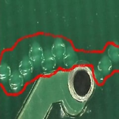
Problem Description: Insufficient air knife pressure or foreign matter in the hole causes tin plug hole Accepted standards: 1. Component holes are not acceptable; 2. SMT BGA vias are not acceptable; 3. Via plugs at other locations are acceptable if they are not higher than the pads. |
 |
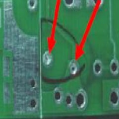
Problem Description: White spots on the board surface may occur due to tin spraying hitting the board, multiple rework or excessive temperature. Accepted standards: 1. The wire spacing is not lower than the minimum wire spacing value; 2. The distance between white spots does not exceed 50% of the distance between the conductive patterns of adjacent non-commonly connected circuits; 3. The white spots on the edge of the board will not reduce the minimum distance between the edge of the board and the conductive pattern; if not specified, it shall not be greater than 2.5MM; 4. The simulated thermal test is not expanded. |
 |
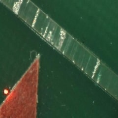
Problem Description:Excessive micro-etching may be caused by too much micro-etching, too many times of tin spraying rework or too slow micro-etching speed. Accepted standards: Not accepted |
 |
Problem Description: The tin spray air knife is scratched or the employee's improper operation causes scratches. Accepted standards: The abrasion area should be within 6.35mm*6.35mm, and there should be no more than 3-5 scratches on the same side. |
 Email: all@poe-pcba.com
 Whatsapp: 85292069596
 Tel: 0755-25312250/ +8613798543496
 Factory Address: Floor 3, Jinyuan Industrial Park, No. 56, Tangtou Avenue, Shiyan Town, Baoan District, Shenzhen China


