
 |
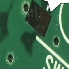
Problem Description: Wrong color of gold. Accepted standards: Not accepted |
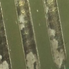 |
Problem Description: Failure to evenly cover Accepted standards: Not accepted |
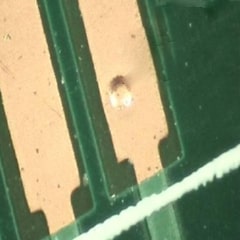 |
Problem Description: The outer layer had dents before gold plating due to human manipulation. Accepted standards: 1. No dents larger than 0.125 mm are allowed in important areas; 2. No dents larger than 0.25 mm are allowed in non-important areas. |
 |
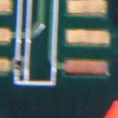
Problem Description: 1. The gold surface is contaminated; 2. Insufficient maintenance; 3. The storage time exceeds the time specified in the document. Accepted standards: Not accepted |
 |
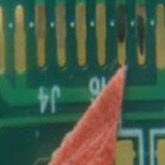
Problem Description: 1. The copper surface debris was not cleaned up during pre-treatment; 2. The nickel cylinder was not activated well. Accepted standards: Not accepted |
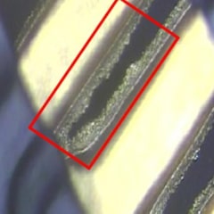 |
Problem Description: 1. Abnormal gold sinking parameters; 2. High concentration and high temperature of the chemical solution; 3. High nickel-gold content; 4. Staying in the tank for too long. Accepted standards: It is acceptable within the range of ±20% of the original spacing, or not exceeding 0.05mm (the smaller of the two). |
 Email: all@poe-pcba.com
 Whatsapp: 85292069596
 Tel: 0755-25312250/ +8613798543496
 Factory Address: Floor 3, Jinyuan Industrial Park, No. 56, Tangtou Avenue, Shiyan Town, Baoan District, Shenzhen China


