5 common mistakes in SMT welding
21 January 2025
Views: 1319
It has become more and more convenient for PCBA manufacturers to make SMT patches. Since engineers have different majors in Chengdu, some engineers will find short circuits or open circuits after receiving the proof boards and cannot test normally. They cannot determine whether there is a problem with their own design or because of Due to factory manufacturing, this wastes a lot of time. Here are 5 of the more common mistakes.
1.The phenomenon of components standing up
The main reason for this occurrence is that the wetting force at both ends of the component is unbalanced, which causes the torque at both ends of the component to be unbalanced.
What situation will cause the wetting force at both ends of the component to be unbalanced during reflow soldering, causing the component to stand up?
1.The pad design and layout are unreasonable;
2.There are problems with solder paste and solder paste printing;
3.The patch is displaced and the force in the Z-axis direction is uneven;
4.The furnace temperature curve is incorrect.
2.Tin beads
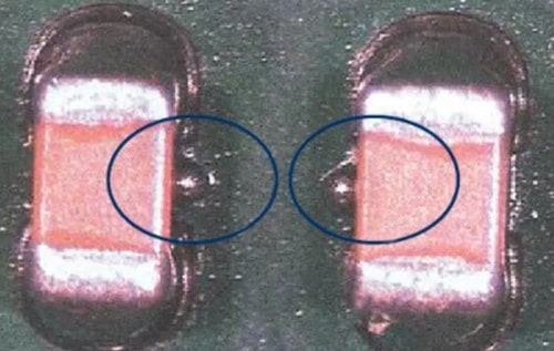
Tin beads are one of the common defects in reflow soldering, which not only affects the appearance but also causes bridging. Tin beads can be divided into two categories: one type appears on one side of the chip component, often in the shape of an independent large ball (as shown below); the other type appears around the IC pins in the shape of scattered beads. The main causes of tin beads are as follows:
1.The temperature curve is incorrect;
2.The quality of the solder paste;
3.The printing is too thick and excess solder paste overflows after the component is pressed down;
4.The pressure on the patch is too great, and the downward pressure causes the solder paste to collapse onto the ink;
5.The shape of the solder pad opening is not good and no anti-tin ball treatment is done;
6.The solder paste has poor activity, dries too quickly, or contains too many small particles of tin powder;
7.The printing is offset, causing part of the solder paste to stick to the PCB;
8.The scraper speed is too fast, causing poor edge sag and the formation of solder balls after reflow.
3.Bridge connection
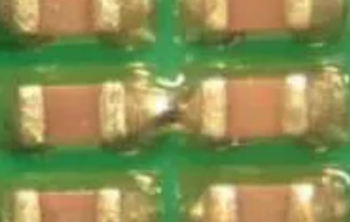
Bridging is also one of the common defects in SMT production. It can cause short circuits between components, and must be repaired if bridging is encountered. The causes of bridging are:
1.Solder paste quality issues;
2.Printing system;
3.The application pressure is too high;
4.The reflow oven heats up too quickly and the solvent in the solder paste does not have time to evaporate.
>
4.Wicking phenomenon
Wicking phenomenon, also known as material sucking phenomenon and core pulling phenomenon, is one of the common welding defects of SMT, which is mostly seen in vapor phase reflow soldering. The solder breaks away from the pad and travels up the pin to between the pin and the chip body, causing serious soldering.

Wicking: refers to the molten solder moistening the component pins and flowing upwards away from the PCB pad area. It is not wetted or partially wetted with the PCB pad, resulting in an open circuit or insufficient solder joint strength. This defect often occurs In devices with wing-shaped leads and J-shaped leads such as QFP, SOP, and PLCC. The wicking phenomenon usually occurs because the thermal conductivity of the pin is too large and the temperature rises rapidly, so that the solder preferentially wets the pin. The wetting force between the solder and the pin is much greater than the wetting force between the solder and the pad. The pin The upward warping will aggravate the occurrence of wicking phenomenon.
5.Poor BGA welding
BGA: Ball Grid Array (ball grid array package). Due to its obvious advantages, BGA packaging has unique advantages in packaging density, electrical performance and cost, allowing it to replace traditional packaging methods. As the market's requirements for chip integration increase, integrated circuit packaging becomes more stringent. The states usually generated are:
1. Connected tin, connected tin is also called a short circuit, that is, the solder ball and the solder ball are short-circuited during the soldering process, causing the two pads to be connected, causing a short circuit.
2. False soldering. False soldering is also called the "Head-in-Pillow (HIP)". There are many reasons for false soldering (oxidation of solder balls or PAD, insufficient temperature in the furnace, PCB deformation, and low solder paste activity). poor etc.). The characteristics of BGA fake soldering are "difficult to find" and "difficult to identify". Named after the shape of a person resting his head on a pillow, the "pillow effect" is a typical and unique failure mode of BGA packaging.
The above are 5 common errors that are easily encountered during SMT processing. Each problem will require methods to solve. Only by finding out the problematic parts of the PCB can we optimize and iterate better.


