
 |
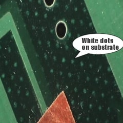
Problem description: There are white spots on the substrate |
| Acceptance Criteria: White spots on the substrate are acceptable for all products except those used in high pressure areas. | |
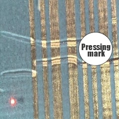 |
Problem description:The steel plate was not cleaned properly when pressing the plate or the sliding plate caused dents. |
| Acceptance Criteria: 1. If the line position exceeds the repair criteria, it must be scrapped; 2. The defect length on the large copper surface is <7mm and each unit does not exceed one line. |
|
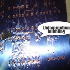 |
Problem description:The copper foil is poorly bonded to the prepreg, resulting in delamination and blistering. |
| Acceptance Criteria: 1. The area affected by the defect does not exceed 1% of the area of each side of the board; 2. The defect does not reduce the spacing between conductive patterns to below the specified minimum spacing requirement; 3. The blistering or delamination span is not greater than 25% of the distance between adjacent conductive patterns; 4. The simulated thermal test is not expanded. |
|
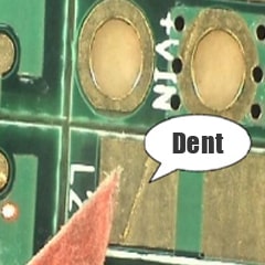 |
Problem description:The steel plate was not cleaned properly or was uneven when pressing the plate, causing dents. |
| Acceptance Criteria: 1. If the line position exceeds the repair criteria, it must be scrapped; 2. If the defect length on the large copper surface is less than 7mm and each unit does not exceed one, it is acceptable. |
 Email: all@poe-pcba.com
 Whatsapp: 85292069596
 Tel: 0755-25312250/ +8613798543496
 Factory Address: Floor 3, Jinyuan Industrial Park, No. 56, Tangtou Avenue, Shiyan Town, Baoan District, Shenzhen China


